Handbook of VLSI Microlithography: Principles, Technology and Applications » książka
topmenu
Handbook of VLSI Microlithography: Principles, Technology and Applications
ISBN-13: 9780815512813 / Angielski / Twarda / 1991 / 671 str.
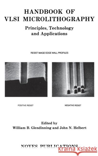
This handbook gives readers a close look at the entire technology of printing very high resolution and high density integrated circuit (IC) patterns into thin resist process transfer coatings-- including optical lithography, electron beam, ion beam, and x-ray lithography. The book's main theme is the special printing process needed to achieve volume high density IC chip production, especially in the Dynamic Random Access Memory (DRAM) industry.
The book leads off with a comparison of various lithography methods, covering the three major patterning parameters of line/space, resolution, line edge and pattern feature dimension control. The book's explanation of resist and resist process equipment technology may well be the first practical description of the relationship between the resist process and equipment parameters. The basics of resist technology are completely covered -- including an entire chapter on resist process defectivity and the potential yield limiting effect on device production. Each alternative lithographic technique and testing method is considered and evaluated: basic metrology including optical, scanning-electron-microscope (SEM) techniques and electrical test devices, along with explanations of actual printing tools and their design, construction and performance. The editor devotes an entire chapter to today's sophisticated, complex electron-beam printers, and to the emerging x-ray printing technology now used in high-density CMOS devices. Energetic ion particle printing is a controllable, steerable technology that does not rely on resist, and occupies a final section of the handbook.


