• Wyszukiwanie zaawansowane
  • Kategorie
  • Kategorie BISAC
  • Książki na zamówienie
  • Promocje
  • Granty
  • Książka na prezent
  • Opinie
  • Pomoc
  • Załóż konto
  • Zaloguj się

Digital CMOS Circuit Design » książka

zaloguj się | załóż konto
Logo Krainaksiazek.pl

koszyk

konto

szukaj
topmenu
Księgarnia internetowa
Szukaj
Książki na zamówienie
Promocje
Granty
Książka na prezent
Moje konto
Pomoc
 
 
Wyszukiwanie zaawansowane
Pusty koszyk
Bezpłatna dostawa dla zamówień powyżej 20 złBezpłatna dostawa dla zamówień powyżej 20 zł

Kategorie główne

• Nauka
 [2950560]
• Literatura piękna
 [1849509]

  więcej...
• Turystyka
 [71097]
• Informatyka
 [151150]
• Komiksy
 [35848]
• Encyklopedie
 [23178]
• Dziecięca
 [617388]
• Hobby
 [139064]
• AudioBooki
 [1657]
• Literatura faktu
 [228597]
• Muzyka CD
 [383]
• Słowniki
 [2855]
• Inne
 [445295]
• Kalendarze
 [1464]
• Podręczniki
 [167547]
• Poradniki
 [480102]
• Religia
 [510749]
• Czasopisma
 [516]
• Sport
 [61293]
• Sztuka
 [243352]
• CD, DVD, Video
 [3414]
• Technologie
 [219456]
• Zdrowie
 [101002]
• Książkowe Klimaty
 [124]
• Zabawki
 [2311]
• Puzzle, gry
 [3459]
• Literatura w języku ukraińskim
 [254]
• Art. papiernicze i szkolne
 [8079]
Kategorie szczegółowe BISAC

Digital CMOS Circuit Design

ISBN-13: 9781461294092 / Angielski / Miękka / 2011 / 384 str.

Silvia Annaratone
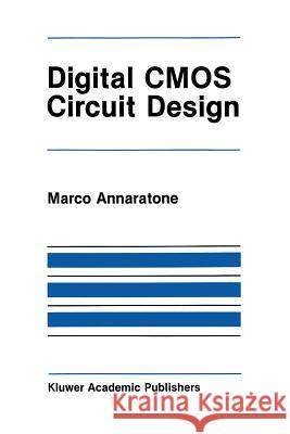
Digital CMOS Circuit Design Silvia Annaratone 9781461294092 Springer - książkaWidoczna okładka, to zdjęcie poglądowe, a rzeczywista szata graficzna może różnić się od prezentowanej.

Digital CMOS Circuit Design

ISBN-13: 9781461294092 / Angielski / Miękka / 2011 / 384 str.

Silvia Annaratone
cena 200,77
(netto: 191,21 VAT:  5%)

Najniższa cena z 30 dni: 192,74
Termin realizacji zamówienia:
ok. 22 dni roboczych
Dostawa w 2026 r.

Darmowa dostawa!

In light of decreasing feature size and greater sophistication of modern processing technology, CMOS has become increasingly attractive, pro viding low-power (at moderate frequencies), good scalability, and rail-to rail operation. For many designers, particularly those approaching VLSI from a system viewpoint, previous experience has been mainly with ratioed NMOS design, and so there is a need to buildon this experienceand make a naturaltransition into CMOS design. Indeed, there ismuch that can bebor rowed from NMOS experience, mainly centered around the techniques for creating N channel pulldown structures. Based on these contributions, CMOS has now grown to the point where there are several circuit styles which have evolved, and these are amply described in this book. Starting at the level ofthe individual MOSFET, basic building blocks are described, as well as the variety of CMOS fabrication processes in contemporary usage. Circuit style issues are then expandedto providethe user with several useful design methodologies, andmuchcareisgiventoelectricalperformancecon siderations, including characteristics of interconnect, gate delay, and I/O buffering. This understanding is then applied to macro-sized components, including array multipliers, where the reader acquires a unified view of ar chitectural performance through parallelism, and circuit performance through scrupulousattentionto device sizingandcontrolofparasiticcircuit elements. In addition, layout techniques to avoid latchup, a consideration not previously encountered by NMOS designers, are given careful treatment.

Kategorie:
Technologie
Kategorie BISAC:
Technology & Engineering > Electrical
Wydawca:
Springer
Seria wydawnicza:
Springer International Series in Engineering and Computer Sc
Język:
Angielski
ISBN-13:
9781461294092
Rok wydania:
2011
Wydanie:
Softcover Repri
Numer serii:
000348000
Ilość stron:
384
Waga:
0.59 kg
Wymiary:
23.5 x 15.5
Oprawa:
Miękka
Wolumenów:
01
Dodatkowe informacje:
Wydanie ilustrowane

1. Introduction.- 1.1. From nMOS to CMOS.- 1.2. CMOS Basic Gates.- 2. MOS Transistor Characteristics.- 2.1. The MOS Transistor.- 2.2. Parasitic Parameters.- 2.3. Small Geometry MOS Transistor.- 2.4. CMOS Transmission Gate.- 2.5. CMOS Inverter.- 2.6. A More Accurate Model for the CMOS Inverter.- 2.7. CMOS Power Dissipation.- 3. Fabrication Processes.- 3.1. The p-well Fabrication Process.- 3.2. The n-well Fabrication Process.- 3.3. LOCMOS Technology.- 3.4. Latchup.- 3.5. The Twin-tub Fabrication Process.- 3.6. The SOS Fabrication Process.- 3.7. Bulk vs. SOI.- 3.8. Design Rules.- 4. Logic Design.- 4.1. Static Logic.- 4.1.1. Complementary Logic.- 4.1.2. nMOS-like Logic.- 4.1.3. Transmission Gate Intensive Logic.- 4.1.4. Cascode Logic.- 4.2. Dynamic Logic.- 4.2.1. Ripple-through Logic.- 4.2.2. P-ELogic.- 4.2.3. Clocked CMOS Logic.- 4.2.4. Domino Logic.- 4.2.5. NORA Logic.- 4.3. Charge Sharing.- 4.4. Bootstrap Logic.- 4.5. Logic Design at the System Level.- 5. Circuit Design.- 5.1. Resistance, Capacitance, and Inductance.- 5.1.1. Interconnect Resistance.- 5.1.2. Interconnect Capacitance.- 5.1.3. Interconnect Inductance.- 5.1.4. Interconnect Discontinuities.- 5.1.5. Coupling Parameters and Interconnect Delay.- 5.1.6. Diffusion Resistance.- 5.1.7. Contact Resistance.- 5.2. Modeling Long Interconnects.- 5.3. The Concept of Equivalent Gate Load.- 5.4. Delay Minimization.- 5.4.1. Inverter Delay and Sizing.- 5.4.2. Inverter Chain Sizing.- 5.4.3. Inverter Chain Sizing with Stray Capacitance.- 5.5. Transistor Sizing in Static Logic.- 5.6. Transistor Sizing in Dynamic Logic.- 6. Design of Basic Circuits.- 6.1. Storage Elements.- 6.2. Full-adder.- 6.3. Programmable Logic Array.- 6.4. Random-access Memory.- 6.4.1. Memory Cell.- 6.4.2. Decoder.- 6.4.3. Sense Amplifier.- 6.5. Parallel Adder.- 6.6. Parallel Multiplier.- 6.6.1. The Design of a Multiplier Based on the Modified Booth Algorithm.- 6.6.2. Basic Building-blocks Inside the Array.- 6.6.3. The Problem of Sign Extension.- 6.6.3.1. The “Sign Propagate” Method.- 6.6.3.2. The “Sign Generate” Method.- 6.6.4. The Implementation of a 24-bit CMOS Booth Multiplier.- 7. Driver and I/O Buffer Design.- 7.1. CMOS Inverter Delay Estimation.- 7.1.1. Fall-time Delay Estimation.- 7.1.1.1. Region 1: n-channel Device in Saturation.- 7.1.1.2. Region 2: n-channel Device in Linear Region.- 7.1.2. Rise-time Delay Estimation.- 7.1.3. Refining the Model.- 7.2. Input Buffer.- 7.3. Output Buffer.- 7.4. Tri-state Output Buffer and I/O Buffer.- 7.5. Output Buffer and Bus Driver Design Optimization.- 7.5.1. Unconstrained Delay Minimization.- 7.5.2. Constrained Delay Minimization.- 7.6. Input Protection.- 7.7. Output Protection.- 7.8. Driving Large On-chip Loads.- Appendix A. Layout.- A. 1. General Considerations on Layout.- A.2. Layout Methodologies for Latchup Avoidance.- A.3. Layout with Structured Methodologies.- A. 4. Power and Ground Routing.- Appendix B. Interconnect Capacitance Computation.- B. 1. Case 1: Coupled Microstrip Structure.- B.2. Case 2: Coupled Stripline Structure.- Appendix C. Figures from Section 5.4.2.- Appendix D. Delay Minimization Based on Eq. (7-3).- Appendix E. Equations Related to Fig. 7-10.- Appendix F. Symbols and Physical Constants.


Udostępnij

Facebook - konto krainaksiazek.pl


Opinie o Krainaksiazek.pl na Opineo.pl

Partner Mybenefit

Krainaksiazek.pl w programie rzetelna firma Krainaksiaze.pl - płatności przez paypal

Czytaj nas na:

Facebook - krainaksiazek.pl
  • książki na zamówienie
  • granty
  • książka na prezent
  • kontakt
  • pomoc
  • opinie
  • regulamin
  • polityka prywatności

Zobacz:

  • Księgarnia czeska

  • Wydawnictwo Książkowe Klimaty

1997-2025 DolnySlask.com Agencja Internetowa

© 1997-2022 krainaksiazek.pl
     
KONTAKT | REGULAMIN | POLITYKA PRYWATNOŚCI | USTAWIENIA PRYWATNOŚCI
Zobacz: Księgarnia Czeska | Wydawnictwo Książkowe Klimaty | Mapa strony | Lista autorów
KrainaKsiazek.PL - Księgarnia Internetowa
Polityka prywatnosci - link
Krainaksiazek.pl - płatnośc Przelewy24
Przechowalnia Przechowalnia