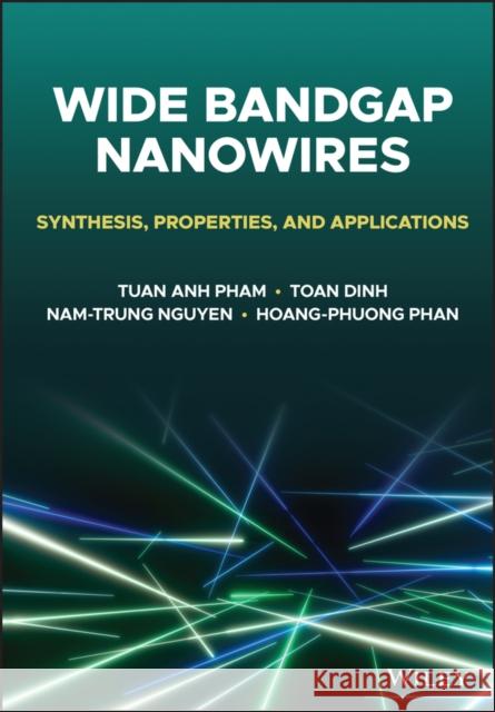
Wide Bandgap Nanowires: Synthesis, Properties, and Applications » książka


Wide Bandgap Nanowires: Synthesis, Properties, and Applications
ISBN-13: 9781119774372 / Angielski / Twarda / 2022 / 288 str.
Wide Bandgap Nanowires: Synthesis, Properties, and Applications
ISBN-13: 9781119774372 / Angielski / Twarda / 2022 / 288 str.
(netto: 703,59 VAT: 5%)
Najniższa cena z 30 dni: 718,04
ok. 30 dni roboczych.
Darmowa dostawa!
Chapter 1 8Bottom-up growth methods 8Abstract 81.1. Introduction 91.2. Bottom-up growth mechanisms 101.2.1. Vapor-liquid-solid growth mechanism 101.2.2. Vapor-solid-solid growth mechanism 161.2.3. Vapor-solid growth mechanism 221.2.4. Solution-liquid-solid growth mechanism 261.3. Bottom-up growth techniques 291.3.1. Chemical Vapor Deposition 291.3.2. Metal-organic chemical vapor deposition 331.3.3. Plasma-enhanced chemical vapor deposition 361.3.4. Hydride vapor phase epitaxy 381.3.5. Molecular Beam Epitaxy 411.3.6. Laser ablation 441.3.7. Thermal evaporation 461.3.8. Carbothermal reduction 48References 51Chapter 2 65Top-down fabrication processes 65Abstract 652.1. Introduction 662.2. Top-down fabrication techniques 682.2.1. Focused ion beam 682.2.2. Electron beam lithography 692.2.3. Reactive ion etching 722.2.4. Combined lithography techniques 74References 76Chapter 3 81Hybrid fabrication techniques and nanowire heterostructures 81Abstract 813.1. Introduction 823.2. Bottom-up meets top-down approaches 843.3. Integration of nanowires onto unconventional substrates 863.3.1. Transferring nanowires onto flexible substrates 863.3.2. Growing nanowires on graphene and layered material substrates 923.4. Synthesis of nanowire heterostructures 953.4.1. Synthesis of one-dimensional heterostructures 953.4.2. Synthesis of mixed dimensional heterostructures 98References 101Chapter 4 108Electrical properties of wide bandgap nanowires 108Abstract 1084.1. Electrical properties 1094.2. Measurement of electrical conductivity 1094.3. Fundamental electrical properties of nanowires 1124.3.1 Effect of doping on electrical properties 1134.3.2 Mobility 1154.3.3 Activation/ionization energy 1164.3.4 Dependence of activation/ionization energy on NW dimensions 1184.4 Electrical properties of wide bandgap nanowire based devices 1184.4.1 Single NW electrical sensing devices 1184.4.2 Field-effect transistors (FETs) 120References 129Chapter 5 132Mechanical properties of wide bandgap nanowires 132Abstract 1325.1. Characterization techniques 1335.1.1 Bending and buckling methods 1335.1.2 Nano indenting method 1385.1.3 Resonance testing method 1395.2. Impact of defects and microstructures on mechanical properties of NWs 1405.2.1. Defects 1405.2.2 Effect of structures, dimensions and temperatures 1435.3. Anelasticity and plasticity properties 1485.3.1 Anelasticity 1485.3.2 Plasticity 1485.3.3 Brittle to ductile transition 150References 152Chapter 6 155Optical properties of wide bandgap nanowires 155Abstract 1556.1 Optical properties of WBG NWs 1566.1.1 Photoluminescence characterization of NWs 1566.1.2 Size-dependent optical properties 1576.1.3 Shape/morphology-dependent optical properties 1586.1.4 Effect of crystal orientation 1596.1.5 Tuning optical properties of NWs 1606.2 Wide bangap nanowire light-emitting diodes (LEDs) 1646.2.1 GaN nanowire based LEDs 1646.2.2 GaN nanowire UV LEDs 1696.2.3 ZnO nanowire based LEDs 172References 175Chapter 7 180Thermal properties of wide bandgap nanowires 180Abstract 1807.1. Thermal conductivity 1817.1.1 Fundamental of thermal transport and thermal conductivity 1817.1.2 Measurement of thermal conductivity 1827.1.3 Effect of diameters on thermal properties 1837.1.4 Effect of orientation on thermal properties 1867.1.5 Tenability of thermal properties 1877.2 Thermoelectric properties 1907.2.1 Fundamental thermoelectric properties 1907.2.2 Thermoelectric properties of ZnO and GaN NWs 1917.2.3 Thermoelectric properties of SiC NWs 1937.2.4 Optimisation of the thermoelectric properties 194References 196Chapter 8 200Ultraviolet sensors 200Abstract 2008.1. Introduction 2018.2. Sensing mechanism 2018.2.1. Photoconductor architectures 2028.2.2. Schottky diode photo sensors 2048.2.3. Semiconductor p-n junction 2068.2.4. Field effect transistor-based UV sensors 2088.3. Device development technologies 2108.3.1. The choice of wide band gap materials for UV sensing 2108.3.2 Top down fabrication of wide band gap nanowire UV sensors 2168.3.4. Transfer process for nanowires 2198.4. Applications of nanowire UV sensors 2228.4.1 Flame sensors 2228.4.2. Environmental monitoring 2248.4.4 Biological sensors and health care applications 225References 227Chapter 9 233Mechanical Sensors 233Abstract 2339.1. Introduction 2349.2. Sensing mechanisms and corresponding materials 2349.2.1. The piezoresistive effect 2349.2.2. Piezotronics effect in nanowires 2399.2.3 Capacitive sensing 2439.3. Transducer configurations and fabrication technologies 2449.3.1. Strain sensors 2449.3.2. Pressure sensors 2489.3.3 Tactile sensors 2539.3.4. Acceleration and vibration sensors 2569.3.5. Energy harvesting devices 2579.4. Applications of mechanical sensors using wide band gap materials 2619.4.1. Structural heath monitoring 2619.4.2. Advanced health care 2629.4.3 Robotics 265References 267Chapter 10 273Gas sensors 273Abstract 27310.1. Introduction 27410.2. Principle of gas sensing 27410.2.1. Transconductance sensing mechanism 27410.2.2. Field effect transistor-based gas sensors 27610.2.3. Metal-semiconductor Schottky contact based gas sensors 27710.2.4. Integration of nanowires with micro heaters 27810.3. Standard physical parameters for gas sensors 28010.3.1. Sensitivity 28010.3.2. Selectivity 28110.3.3. Response time 28210.4. Materials for different types of gases 28410.4.1 Oxygen sensors 28410.4.2 Carbon dioxide 28510.4.3 Organic gases 28710.4.4 Hydrogen gas 290References 301Chapter 11 308Wide band gap nanoresonators 308Abstract 30811.1. Introduction 30911.2. Principle of nanoresonators 31011.3. Actuation and measurement techniques 31611.3.1 Electrostatic actuation 31611.3.2 Piezoelectric actuation 31811.3.3 Magnetomotive actuation 32011.3.4. Thermal actuator 32311.4. Engineering the performance of nanoresonators using wide band gap materials 32511.4.1. Residual stress 32511.4.2 Mechanical clamping enhancement 32911.4.3 Tunning resonant frequency using electrically driven forces 33111.5. Applications of nanoresonators 33411.5.1 Logic Circuit at high temperatures 33411.5.2 Mass sensing applications 33711.5.3 Biosensors 33811.5.4 Mechanical sensing 33911.5.5 Optical devices 341References 343
Tuan Anh Pham is a research assistant as well as a process engineer at the Queensland Micro- and Nanotechnology Centre, Griffith University, Australia. Dr. Pham's longstanding research interests have been focused on various fields of condensed matter physics and materials science, including 1D/2D materials, topological insulators, wide bandgap semiconductors, surface science, and wearable technology.Toan Dinh is a Senior Lecturer in the School of Engineering, University of Southern Queensland, Australia. Dr. Dinh's research interests include micro/nano-electromechanical systems (MEMS/NEMS), physics of semiconductors, sensors for harsh environments, soft robotics, and advanced materials for healthcare and wearable applications.Nam-Trung Nguyen is a Professor and the Director of Queensland Micro- and Nanotechnology Centre at Griffith University in Brisbane, Australia, and leads a research group of over 20 postgraduate and postdoctoral researchers. Research themes of the group include micro- and nanofluidics, micro- and nanofabrication; as well as micro- electromechanical systems (MEMS).Hoang-Phuong Phan is currently an ARC DECRA Fellow at Queensland Micro- and Nanotechnology Centre, Griffith University. He will join the University of New South Wales (UNSW), Sydney, Australia from March 2022 as a Senior Lecturer. The Phan Lab's research interest covers a broad range of semiconductor devices and applications, including MEMS/NEMS, integrated sensors, flexible electronics, and bio-sensing applications.
1997-2026 DolnySlask.com Agencja Internetowa
KrainaKsiazek.PL - Księgarnia Internetowa


