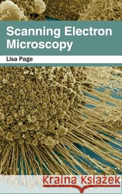
Scanning Electron Microscopy » książka
Scanning Electron Microscopy
ISBN-13: 9781632384065 / Angielski / Twarda / 2015 / 292 str.
Fine focused electron and ion beams constitute(s) an inevitable part of methods and instruments employed in various science fields. SEMs are well instrumented and supplemented with advanced techniques and methods and thereby present endless possibilities in the areas of quantitative measurement of object topologies, surface imaging, performing elemental analysis and local electrophysical characteristics of semiconductor structures. Creation of micro and nanostructures involves extensive use of fine focused e-beam. This book focuses on various issues concerned with scanning electron microscopy, covering both theoretical and practical aspects. Numerous topics are organized under two sections, "Material Science" and "Nanostructured Materials for Electronic Industry." This book includes contributions by renowned researchers and experts in this field.
Fine focused electron and ion beams constitute(s) an inevitable part of methods and instruments employed in various science fields. SEMs are well instrumented and supplemented with advanced techniques and methods and thereby present endless possibilities in the areas of quantitative measurement of object topologies, surface imaging, performing elemental analysis and local electrophysical characteristics of semiconductor structures. Creation of micro and nanostructures involves extensive use of fine focused e-beam. This book focuses on various issues concerned with scanning electron microscopy, covering both theoretical and practical aspects. Numerous topics are organized under two sections, "Material Science" and "Nanostructured Materials for Electronic Industry". This book includes contributions by renowned researchers and experts in this field.


