• Wyszukiwanie zaawansowane
  • Kategorie
  • Kategorie BISAC
  • Książki na zamówienie
  • Promocje
  • Granty
  • Książka na prezent
  • Opinie
  • Pomoc
  • Załóż konto
  • Zaloguj się

Dielectric Films for Advanced Microelectronics » książka

zaloguj się | załóż konto
Logo Krainaksiazek.pl

koszyk

konto

szukaj
topmenu
Księgarnia internetowa
Szukaj
Książki na zamówienie
Promocje
Granty
Książka na prezent
Moje konto
Pomoc
 
 
Wyszukiwanie zaawansowane
Pusty koszyk
Bezpłatna dostawa dla zamówień powyżej 20 złBezpłatna dostawa dla zamówień powyżej 20 zł

Kategorie główne

• Nauka
 [2946600]
• Literatura piękna
 [1856966]

  więcej...
• Turystyka
 [72221]
• Informatyka
 [151456]
• Komiksy
 [35826]
• Encyklopedie
 [23190]
• Dziecięca
 [619653]
• Hobby
 [140543]
• AudioBooki
 [1577]
• Literatura faktu
 [228355]
• Muzyka CD
 [410]
• Słowniki
 [2874]
• Inne
 [445822]
• Kalendarze
 [1744]
• Podręczniki
 [167141]
• Poradniki
 [482898]
• Religia
 [510455]
• Czasopisma
 [526]
• Sport
 [61590]
• Sztuka
 [243598]
• CD, DVD, Video
 [3423]
• Technologie
 [219201]
• Zdrowie
 [101638]
• Książkowe Klimaty
 [124]
• Zabawki
 [2473]
• Puzzle, gry
 [3898]
• Literatura w języku ukraińskim
 [254]
• Art. papiernicze i szkolne
 [8170]
Kategorie szczegółowe BISAC

Dielectric Films for Advanced Microelectronics

ISBN-13: 9780470013601 / Angielski / Twarda / 2007 / 512 str.

Mikhail Baklanov; Martin Green; Karen Maex
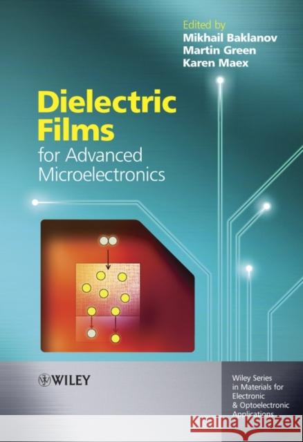
Dielectric Films for Advanced Microelectronics Mikhail Baklanov Martin Green Karen Maex 9780470013601 John Wiley & Sons - książkaWidoczna okładka, to zdjęcie poglądowe, a rzeczywista szata graficzna może różnić się od prezentowanej.

Dielectric Films for Advanced Microelectronics

ISBN-13: 9780470013601 / Angielski / Twarda / 2007 / 512 str.

Mikhail Baklanov; Martin Green; Karen Maex
cena 1132,15 zł
(netto: 1078,24 VAT:  5%)

Najniższa cena z 30 dni: 1122,87 zł
Termin realizacji zamówienia:
ok. 30 dni roboczych
Bez gwarancji dostawy przed świętami

Darmowa dostawa!

The topic of thin films is an area of increasing importance in materials science, electrical engineering and applied solid state physics; with both research and industrial applications in microelectronics, computer manufacturing, and physical devices. Advanced, high-performance computers, high-definition TV, broadband imaging systems, flat-panel displays, robotic systems, and medical electronics and diagnostics are a few examples of the miniaturized device technologies that depend on the utilization of thin film materials. This book presents an in-depth overview of the novel developments made by the scientific leaders in the area of modern dielectric films for advanced microelectronic applications. It contains clear, concise explanations of material science of dielectric films and their problem for device operation, including high-k, low-k, medium-k dielectric films and also specific features and requirements for dielectric films used in the packaging technology. A broad range of related topics are covered, from physical principles to design, fabrication, characterization, and applications of novel dielectric films.

Kategorie:
Nauka, Chemia
Kategorie BISAC:
Technology & Engineering > Materials Science - Thin Films, Surfaces & Interfaces
Technology & Engineering > Electrical
Technology & Engineering > Electronics - Microelectronics
Wydawca:
John Wiley & Sons
Seria wydawnicza:
Wiley Series in Materials for Electronic and Optoelectronic
Język:
Angielski
ISBN-13:
9780470013601
Rok wydania:
2007
Numer serii:
000298427
Ilość stron:
512
Waga:
1.09 kg
Wymiary:
24.92 x 17.42 x 3.38
Oprawa:
Twarda
Wolumenów:
01
Dodatkowe informacje:
Bibliografia
Wydanie ilustrowane

"The book is well organized and has excellent technical depth with recent state–of–the–art information. Researchers, graduate students, and those in industry working on finding new materials and processes for thin–film dielectric materials would find this book to be a valuable resource." ( IEEE Electrical Insulation Magazine, March/April 2009)

Series Preface. Preface. (Mikhail Baklanov, Martin Green and Karen Maex) . 1. Low and Ultralow Dielectric Constant Films Prepared by Plasma–Enhanced Chemical Vapor Deposition. (A. Grill) . 2. Spin–On Dielectric Materials. (Geraud Dubois, Willi Volksen and Robert D. Miller) . 3.Porosity of Low Dielectric Constant Materials. 3.1 Positron Annihilation Spectroscopy. (David W. Gidley, Hua–Gen Peng, and Richard Vallery). 3.2 Structure Characterization of Nanoporous Interlevel Dielectric Thin Films with X–ray and Neutron Radiation. (Christopher L. Soles, Hae–Jeong Lee, Bryan D. Vogt, Eric K. Lin, Wen–li Wu) . 3.3 Ellipsometric Porosimetry. (M. R. Baklanov). 4. Mechanical and Transport Properties of Low–k Dielectrics. (J.L. Plawsky, R. Achanta, W. Cho, O. Rodriguez, R. Saxena, and W.N. Gill) . 5. Integration of low–k dielectric films in damascene processes. (R.J.O.M. Hoofman, V.H. Nguyen,V. Arnal, M. Broekaart, L.G. Gosset,W.F.A. Besling, M. Fayolle and F. Iacopi) . 6. ONO structures and oxynitrides in modern microelectronics. Material science, characterization and application. (Yakov  Roizin  and Vladimir  Gritsenko). High Dielectric constant Materials. 7. Material Engineering of High–k Gate Dielectrics. (Akira Toriumi and Koji Kita) . 8. Physical Characterisation of ultra–thin high–k dielectric . (T. Conard, H. Bender and W. Vandervorst) . 9. Electrical Characterization of Advanced Gate Dielectrics. (Robin Degraeve, Jurriaan Schmitz, Luigi Pantisano, Eddy Simoen, Michel Houssa, Ben Kaezer, and Guido Groeseneken) . Medium dielectric constant materials. 10. Integration Issues of High–k Gate Dielectrics. (Yasuo Nara) . Dielectric films for interconnects (packaging). 11. Anisotropic Conductive Film (ACF) for Advanced Microelectronic Interconnects. (Yi Li, C. P. Wong) . Index.

Karen Maex, IMEC Fellow, Silicon Process and Device Technology Division, Leuven, Belgium & Professor at Katholieke Universiteit Leuven

Mikhail R. Baklanov, Principal Scientist, Silicon Process and Device Technology Division, IMEC, Leuven, Belgium

IMEC is the largest independent microelectronics R&D centre in Europe, with over 1250 staff. R&D ranges from the design of complex single–chip and single–package systems for telecommunications and multimedia, new process technologies for optoelectronics, photovoltaics, area–array packing, etc.

The dielectric properties of silicon dioxide (SiO 2), such as high resistivity and excellent dielectric strength, have aided the evolution of microelectronics during the past 40 years. Silica films have been successfully used over this period for both gate and interconnect applications in ultra large–scale integration (ULSI) devices. Dielectric films for gate applications need to have a higher dielectric constant, while interconnect dielectric materials need to have a lower dielectric constant, compared with SiO 2. In order to maintain the high drive current and gate capacitance required of scaled MOSFETs ( metal– oxide– silicon field effect transistors), SiO 2 gate dielectrics have decreased in thickness to less than 2 nm today, with a continued effort to shrink to the thickness below 1 nm. However, SiO 2 layers thinner than 1.2 nm do not have the insulating properties required of a gate dielectric and ultrathin SiO 2 gate dielectrics give rise to a number of problems, such as high gate leakage current and reliability degradation. Therefore, alternative gate dielectric materials are required.

SiO2, having been the universal dielectric material for both gate and interlayer dielectric (ILD) applications for many years, must be replaced by materials with a higher dielectric constant for the gate applications and a reduced dielectric constant for interconnect applications. Replacements for silicon dioxide, such as HfO2, ZrO2, and Al2O3, for introduction as high–k dielectrics (described in the central section of the book), have material properties that are quite different compared with those of traditional dense SiO2 and these differences create many technological challenges that are the subject of intensive research. In addition, not only the development of new gate materials but also re–engineering of many technological processes is needed. For example, in the case of low–k materials (discussed in the first section of the book), active species formed during different technological processes diffuse into the pores and create severe damage. All these problems have been stimulating the development of new technological approaches, which will be dealt with in this book.

This book presents an in–depth overview of novel developments made by scientific leaders in the microelectronics community. It covers a broad range of related topics, from physical principles to design, fabrication, characterization, and application of novel dielectric films. This book is intended for postgraduate level students, PhD students and industrial researchers, to enable them to gain insight into this important area of research.

Green, Martin Green is Professor of English at Tufts University.... więcej >


Udostępnij

Facebook - konto krainaksiazek.pl


Opinie o Krainaksiazek.pl na Opineo.pl

Partner Mybenefit

Krainaksiazek.pl w programie rzetelna firma Krainaksiaze.pl - płatności przez paypal

Czytaj nas na:

Facebook - krainaksiazek.pl
  • książki na zamówienie
  • granty
  • książka na prezent
  • kontakt
  • pomoc
  • opinie
  • regulamin
  • polityka prywatności

Zobacz:

  • Księgarnia czeska

  • Wydawnictwo Książkowe Klimaty

1997-2025 DolnySlask.com Agencja Internetowa

© 1997-2022 krainaksiazek.pl
     
KONTAKT | REGULAMIN | POLITYKA PRYWATNOŚCI | USTAWIENIA PRYWATNOŚCI
Zobacz: Księgarnia Czeska | Wydawnictwo Książkowe Klimaty | Mapa strony | Lista autorów
KrainaKsiazek.PL - Księgarnia Internetowa
Polityka prywatnosci - link
Krainaksiazek.pl - płatnośc Przelewy24
Przechowalnia Przechowalnia