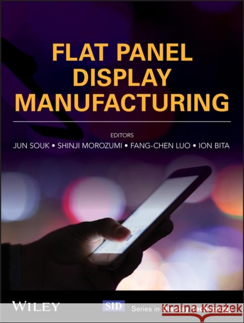
Flat Panel Display Manufacturing » książka


Flat Panel Display Manufacturing
ISBN-13: 9781119161349 / Angielski / Twarda / 2018 / 352 str.
Flat Panel Display Manufacturing
ISBN-13: 9781119161349 / Angielski / Twarda / 2018 / 352 str.
(netto: 631,86 VAT: 5%)
Najniższa cena z 30 dni: 656,68
ok. 30 dni roboczych.
Darmowa dostawa!
An extensive introduction to the engineering and manufacture of current and next–generation flat panel displays
This book provides a broad overview of the manufacturing of flat panel displays, with a particular emphasis on the display systems at the forefront of the current mobile device revolution.
List of Contributors xxi
Series Editor s Foreword xxv
Preface xxvii
1 Introduction 1
Fang –Chen Luo, Jun Souk, Shinji Morozumi, and Ion Bita
1.1 Introduction 1
1.2 Historic Review of TFT –LCD Manufacturing Technology Progress 1
1.3 Analyzing the Success Factors in LCD Manufacturing 5
References 11
2 TFT Array Process Architecture and Manufacturing Process Flow 13
Chiwoo Kim
2.1 Introduction 13
2.2 Material Properties and TFT Characteristics of a –Si, LTPS, and Metal Oxide TFTs 15
2.3 a –Si TFT Array Process Architecture and Process Flow 22
2.4 Poly –Si TFT Architecture and Fabrication 27
2.5 Oxide Semiconductor TFT Architecture and Fabrication 30
2.6 TFT LCD Applications 32
2.7 Development of SLS –Based System on Glass Display [1, 11, 14, 15– 33
References 35
3 Color Filter Architecture, Materials, and Process Flow 39
Young Seok Choi, Musun Kwak, and Youn Sung Na
3.1 Introduction 39
3.2 Structure and Role of the Color Filter 39
3.3 Color Filter Manufacturing Process Flow 46
3.4 New Color Filter Design 55
References 57
4 Liquid Crystal Cell Process 59
Heung –Shik Park and Ki –Chul Shin
4.1 Introduction 59
4.2 Liquid Crystal Cell Process 59
4.3 Conclusions 70
Acknowledgments 70
References 70
5 TFT –LCD Module and Package Process 73
Chun Chang Hung
5.1 Introduction 73
5.2 Driver IC Bonding: TAB and COG 73
5.3 Introduction to Large –Panel JI Process 74
5.4 Introduction to Small –Panel JI Process 79
5.5 LCD Module Assembly 83
5.6 Aging 84
5.7 Module in Backlight or Backlight in Module 85
References 86
6 LCD Backlights 87
Insun Hwang and Jae –Hyeon Ko
6.1 Introduction 87
6.2 LED Sources 90
6.3 Light Guide Plate 98
6.4 Optical Films 104
6.5 Direct –Type BLU 111
6.6 Summary 111
References 112
7 TFT Backplane and Issues for OLED 115
Chiwoo Kim
7.1 Introduction 115
7.2 LTPS TFT Backplane for OLED Films 116
7.3 Oxide Semiconductor TFT for OLED 122
7.4 Best Backplane Solution for AMOLED 125
References 127
8A OLED Manufacturing Process for Mobile Application 129
Jang Hyuk Kwon and Raju Lampande
8A.1 Introduction 129
8A.2 Current Status of AMOLED for Mobile Display 130
8A.2.1 Top Emission Technology 130
8A.3 Fine Metal Mask Technology (Shadow Mask Technology) 133
8A.4 Encapsulation Techniques for OLEDs 135
8A.4.1 Frit Sealing 135
8A.4.2 Thin –Film Encapsulation 136
8A.5 Flexible OLED technology 137
8A.6 AMOLED Manufacturing Process 137
8A.7 Summary 140
References 140
8B OLED Manufacturing Process for TV Application 143
Chang Wook Han and Yoon Heung Tak
8B.1 Introduction 143
8B.2 Fine Metal Mask (FMM) 144
8B.3 Manufacturing Process for White OLED and Color Filter Methods 147
8B.3.1 One –Stacked White OLED Device 149
8B.3.2 Two –Stacked White OLED Device 152
8B.3.3 Three –Stacked White –OLED Device 155
References 157
9 OLED Encapsulation Technology 159
Young –Hoon Shin
9.1 Introduction 159
9.2 Principles of OLED Encapsulation 159
9.2.1 Effect of H2O 160
9.3 Classification of Encapsulation Technologies 162
9.4 Summary 170
References 170
10 Flexible OLED Manufacturing 173
Woojae Lee and Jun Souk
10.1 Introduction 173
10.2 Critical Technologies in Flexible OLED Display 174
10.3 Process Flow of F –OLED 181
10.4 Foldable OLED 186
10.5 Summary 188
References 189
11A Metal Lines and ITO PVD 193
Hyun Eok Shin, Chang Oh Jeong, and Junho Song
11A.1 Introduction 193
11A.1.1 Basic Requirements of Metallization for Display 193
11A.1.2 Thin –Film Deposition by Sputtering 195
11A.2 Metal Line Evolution in Past Years of TFT –LCD 198
11A.2.1 Gate Line Metals 199
11A.2.2 Data line (Source/Drain) Metals 202
11A.3 Metallization for OLED Display 205
11A.3.1 Gate Line Metals 205
11A.3.2 Source/Drain Metals 205
11A.3.3 Pixel Anode 206
11A.4 Transparent Electrode 207
References 208
11B Thin –Film PVD: Materials, Processes, and Equipment 209
Tetsuhiro Ohno
11B.1 Introduction 209
11B.2 Sputtering Method 210
11B.3 Evolution of Sputtering Equipment for FPD Devices 212
11B.3.1 Cluster Tool for Gen 2 Size 212
11B.3.2 Cluster Tool for Gen 4.5 to Gen 7 Size 213
11B.3.3 Vertical Cluster Tool for Gen 8 Size 213
11B.4 Evolution of Sputtering Cathode 215
11B.4.1 Cathode Structure Evolution 215
11B.4.2 Dynamic Multi Cathode for LTPS 217
11B.4.3 Cathode Selection Strategy 217
11B.5 Transparent Oxide Semiconductor (TOS) Thin –Film Deposition Technology 218
11B.5.1 Deposition Equipment for TOS –TFT 218
11B.5.2 New Cathode Structure for TOS –TFT 219
11B.6 Metallization Materials and Deposition Technology 221
References 223
11C Thin –Film PVD (Rotary Target) 225
Marcus Bender
11C. 1 Introduction 225
11C.2 Source Technology 227
11C.2.1 Planar Cathodes 227
11C.2.2 Rotary Cathodes 229
11C.2.3 Rotary Cathode Array 230
11C.3 Materials, Processes, and Characterization 232
11C.3.1 Introduction 232
11C.3.2 Backplane Metallization 232
11C.3.3 Layers for Metal –Oxide TFTs 234
11C.3.4 Transparent Electrodes 236
11C.3.5 Adding Touch Functionality and Improving End –User Experience 238
References 239
12A Thin –Film PECVD (AKT) 241
Tae Kyung Won, Soo Young Choi, and John M. White
12A.1 Introduction 241
12A.2 Process Chamber Technology 243
12A.2.1 Electrode Design 243
12A.2.2 Chamber Cleaning 246
12A.3 Thin –Film Material, Process, and Characterization 248
12A.3.1 Amorphous Si (a –Si) TFT 248
12A.3.2 Low –Temperature Poly Silicon (LTPS) TFT 258
12A.3.3 Metal –Oxide (MO) TFT 263
12A.3.4 Thin –Film Encapsulation (TFE) 269
References 271
12B Thin –Film PECVD (Ulvac) 273
Masashi Kikuchi
12B.1 Introduction 273
12B.2 Plasma of PECVD 273
12B.3 Plasma Modes and Reactor Configuration 273
12B.4 PECVD Process for Display 276
12B.5 PECVD System Overview 279
12B.6 Remote Plasma Cleaning 279
12B.7 Passivation Layer for OLED 282
12B.8 PECVD Deposition for IGZO TFT 283
12B.9 Particle Generation 284
References 286
13 Photolithography 287
Yasunori Nishimura, Kozo Yano, Masataka Itoh, and Masahiro Ito
13.1 Introduction 287
13.2 Photolithography Process Overview 288
13.3 Photoresist Coating 290
13.4 Exposure 292
13.5 Photoresist Development 300
13.6 Inline Photolithography Processing Equipment 301
13.7 Photoresist Stripping 302
13.8 Photolithography for Color Filters 303
References 310
14A Wet Etching Processes and Equipment 311
Kazuo Jodai
14A.1 Introduction 311
14A.2 Overview of TFT Process 312
14A.3 Applications and Equipment of Wet Etching 313
14A.3.1 Applications 313
14A.3.2 Equipment (Outline) 313
14A.3.3 Substrate Transferring System 315
14A.3.4 Dip Etching System 316
14A.3.5 Cascade Rinse System 316
14A.4 Problems Due to Increased Mother Glass Size and Solutions 317
14A.4.1 Etchant Concentration Management 317
14A.4.2 Quick Rinse 317
14A.4.3 Other Issues 318
14A.5 Conclusion 318
References 318
14B Dry Etching Processes and Equipment 319
Ippei Horikoshi
14B.1 Introduction 319
14B.2 Principle of Dry Etching 319
14B.2.1 Plasma 320
14B.2.2 Ions 321
14B.2.3 Radicals 321
14B.3 Architecture for Dry Etching Equipment 322
14B.4 Dry Etching Modes 323
14B.4.1 Conventional Etching Mode and Each Characteristic 324
14B.4.2 Current Etching Mode and Each Characteristic 325
14B.5 TFT Process 325
14B.5.1 a –Si Process 325
14B.5.2 LTPS Process 326
14B.5.3 Oxide Process 327
References 328
15 TFT Array: Inspection, Testing, and Repair 329
Shulik Leshem, Noam Cohen, Savier Pham, Mike Lim, and Amir Peled
15.1 Defect Theory 329
15.2 AOI (Automated Optical Inspection) 334
15.3 Electrical Testing 352
15.4 Defect Repair 363
16 LCM Inspection and Repair 379
Chun Chang Hung 379
16.1 Introduction 379
16.2 Functional Defects Inspection 379
16.3 Cosmetic Defects Inspection 381
16.4 Key Factors for Proper Inspection 383
16.5 Automatic Optical Inspection (AOI) 388
16.6 LCM Defect Repair 388
References 391
17 Productivity and Quality Control Overview 393
Kozo Yano, Yasunori Nishimura, and Masataka Itoh
17.1 Introduction 393
17.2 Productivity Improvement 394
17.3 Yield Management 399
17.4 Quality Control System 406
References 417
18 Plant Architectures and Supporting Systems 419
Kozo Yano and Michihiro Yamakawa
18.1 Introduction 419
18.2 General Issues in Plant Architecture 420
18.3 Clean Room Design 423
18.4 Supporting Systems with Environmental Consideration 433
18.5 Production Control System 437
References 440
19 Green Manufacturing 441
YiLin Wei, Mona Yang, and Matt Chien
19.1 Introduction 441
19.2 Fabrication Plant (Fab) Design 441
19.3 Product Material Uses 443
19.4 Manufacturing Features and Green Management 447
19.5 Future Challenges 453
References 454
Index 457
JUN SOUK, PHD is a Professor in the Department of Electronic Engineering, Hanyang University, South Korea.
SHINJI MOROZUMI, PHD is the founder and chairman of Crystage Inc., Japan.
FANG–CHEN LUO, PHD is advisor to the President and Fellow of AU Optronics, Taiwan.
ION BITA, PHD leads development of display technologies and components at Apple Inc., USA.
AN EXTENSIVE INTRODUCTION TO THE ENGINEERING AND MANUFACTURE OF CURRENT AND NEXT–GENERATION FLAT PANEL DISPLAYS
This book provides a broad overview of the manufacturing of flat panel displays, with a particular emphasis on the display systems at the forefront of the current mobile device revolution. It is structured to cover a broad spectrum of topics within the unifying theme of display systems manufacturing. An important theme of this book is treating displays as systems, which expands the scope beyond the technologies and manufacturing of traditional display panels (LCD and OLED) to also include key components for mobile device applications, such as flexible OLED, thin LCD backlights, as well as the manufacturing of display module assemblies.
Flat Panel Display Manufacturing fills an important gap in the current book literature, describing the state of the art in display manufacturing for today′s displays, and looks to create a reference of the development of next generation displays. The editorial team brings a broad and deep perspective on flat panel display manufacturing, with a global view spanning decades of experience at leading institutions in Japan, Korea, Taiwan, and the USA, and including direct pioneering contributions to the development of displays. The book includes a total of 24 chapters contributed by experts at leading manufacturing institutions from the global FPD industry in Korea, Japan, Taiwan, Germany, Israel, and USA.
- Provides an overview of the evolution of display technologies and manufacturing
- Treats display products as systems with manifold applications, expanding the scope beyond traditional display panel manufacturing to key components for mobile devices and TV applications
- Provides a detailed overview of LCD manufacturing, including panel architectures, process flows, and module manufacturing
- Provides a detailed overview of OLED manufacturing for both mobile and TV applications, including a chapter dedicated to the young field of flexible OLED manufacturing
- Provides a detailed overview of the key unit processes and corresponding manufacturing equipment, including manufacturing test & repair of TFT array panels as well as display module inspection and repair
- Introduces key topics in display manufacturing science and engineering, including productivity and quality, factory architectures, and green manufacturing
Flat Panel Display Manufacturing will appeal to professionals and engineers in R&D departments for display–related technology development, as well as to graduates and Ph.D. students specializing in LCD/OLED/other flat panel displays.
WILEY SID Series in Display Technology
Series Editor: Ian Sage, Abelian Services, Malvern, UK
The Society for Information Display (SID) is an international society which has the aim of encouraging the development of all aspects of the field of information display. Complementary to the aims of the society, the Wiley–SID series is intended to explain the latest developments in information display technology at a professional level. The broad scope of the series addresses all facets of information displays from technical aspects through systems and prototypes to standards and ergonomics.
1997-2026 DolnySlask.com Agencja Internetowa
KrainaKsiazek.PL - Księgarnia Internetowa


