Termin realizacji zamówienia: ok. 22 dni roboczych.
Darmowa dostawa!
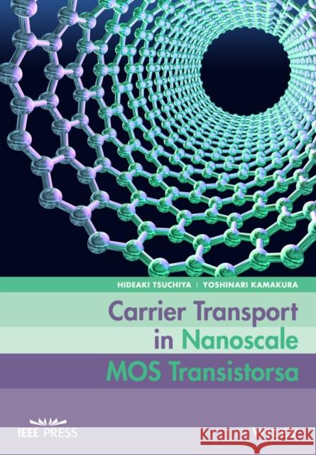
A comprehensive advanced level examination of the transport theory of nanoscale devices
Provides advanced level material of electron transport in nanoscale devices from basic principles of quantum mechanics through to advanced theory and various numerical techniques for electron transport
Combines several up-to-date theoretical and numerical approaches in a unified manner, such as Wigner-Boltzmann equation, the recent progress of carrier transport research for nanoscale MOS transistors, and quantum correction approximations
The authors approach the subject in a logical and systematic way, reflecting their extensive teaching and research backgrounds
2 First –principles calculations for Si nanostructures 12
2.1 Band structure calculations 12
2.1.1 Si ultrathin –body structures 12
2.1.2 Si nanowires 17
2.1.3 Strain effects on band structures: From bulk to nanowire 20
2.2 Tunneling current calculations through Si/SiO2/Si structures 31
2.2.1 Atomic models of Si (001)/SiO2 /Si (001) structures 32
2.2.2 Current –voltage characteristics 33
2.2.3 SiO2 thickness dependences 35
3 Quasi –ballistic Transport in Si Nanoscale MOSFETs 41
3.1 A picture of quasi –ballistic transport simulated using quantum –corrected Monte Carlo simulation 41
3.1.1 Device structure and simulation method 42
3.1.2 Scattering rates for 3 –D electron gas 44
3.1.3 Ballistic transport limit 46
3.1.4 Quasi –ballistic transport 50
3.1.5 Role of elastic and inelastic phonon scattering 51
3.2 Multi –sub –band Monte Carlo simulation considering quantum confinement in inversion layers 55
3.2.1 Scattering Rates for 2 –D Electron Gas 56
3.2.2 Increase in Dac for SOI MOSFETs 58
3.2.3 Simulated electron mobilities in bulk Si and SOI MOSFETs 59
3.2.4 Electrical characteristics of Si DG –MOSFETs 61
3.3 Extraction of quasi –ballistic transport parameters in Si DG –MOSFETs 64
3.3.1 Backscattering coefficient 64
3.3.2 Current drive 66
3.3.3 Gate and drain bias dependences 67
3.4 Quasi –ballistic transport in Si junctionless transistors 69
3.4.1 Device structure and simulation conditions 70
3.4.2 Influence of SR scattering 71
3.4.3 Influence of II scattering 74
3.4.4 Backscattering coefficient 75
3.5 Quasi –ballistic transport in GAA –Si nanowire MOSFETs 76
3.5.1 Device structure and 3DMSB –MC method 76
3.5.2 Scattering rates for 1 –D electron gas 77
3.5.3 ID–VG characteristics and backscattering coefficient 79
4 Phonon Transport in Si Nanostructures 85
4.1 Monte Carlo simulation method 87
4.1.1 Phonon dispersion model 87
4.1.2 Particle simulation of phonon transport 88
4.1.3 Free flight and scattering 89
4.2 Simulation of thermal conductivity 91
4.2.1 Thermal conductivity of bulk silicon 91
4.2.2 Thermal conductivity of silicon thin films 94
4.2.3 Thermal conductivity of silicon nanowires 98
4.2.4 Discussion on Boundary scattering effect 100
4.3 Simulation of heat conduction in devices 102
4.3.1 Simulation method 102
4.3.2 Simple 1 –D structure 103
4.3.3 FinFET structure 106
5 Carrier Transport in High –mobility MOSFETs 112
5.1 Quantum –corrected MC Simulation of High –mobility MOSFETs 112
5.1.1 Device Structure and Band Structures of Materials 112
5.1.2 Band Parameters of Si, Ge, and III –V Semiconductors 114
5.1.3 Polar –optical Phonon (POP) Scattering in III –V Semiconductors 115
5.1.4 Advantage of UTB Structure 116
5.1.5 Drive Current of III –V, Ge and Si n –MOSFETs 119
5.2 Source –drain Direct Tunneling in Ultrascaled MOSFETs 124
5.3 Wigner Monte Carlo (WMC) Method 125
5.3.1 Wigner Transport Formalism 126
5.3.2 Relation with Quantum –corrected MC Method 129
5.3.3 WMC Algorithm 131
5.3.4 Description of Higher –order Quantized Subbands 133
5.3.5 Application to Resonant –tunneling Diode 133
5.4 Quantum Transport Simulation of III –V n –MOSFETs with Multi –subband WMC (MSB –WMC) Method 138
5.4.1 Device Structure 138
5.4.2 POP Scattering Rate for 2 –D Electron Gas 139
5.4.3 ID–VG Characteristics for InGaAs DG –MOSFETs 139
5.4.4 Channel Length Dependence of SDT Leakage Current 143
5.4.5 Effective Mass Dependence of Subthreshold Current Properties 144
6 Atomistic Simulations of Si, Ge and III –V Nanowire MOSFETs 151
6.1 Phonon –limited electron mobility in Si nanowires 151
6.1.1 Band structure calculations 152
6.1.2 Electron –phonon interaction 161
6.1.3 Electron mobility 162
6.2 Comparison of phonon –limited electron mobilities between Si and Ge nanowires 168
6.3 Ballistic performances of Si and InAs nanowire MOSFETs 173
6.3.1 Band structures 174
6.3.2 Top –of –the –barrier model 174
6.3.3 ID–VG characteristics 177
6.3.4 Quantum capacitances 178
6.3.5 Power –delay –product 179
6.4 Ballistic performances of InSb, InAs, and GaSb nanowire MOSFETs 181
6.4.1 Band structures 182
6.4.2 ID–VG characteristics 182
6.4.3 Power –delay –product 186
Appendix A: Atomistic Poisson equation 187
Appendix B: Analytical expressions of electron –phonon interaction Hamiltonian matrices 188
7 2 –D Materials and Devices 191
7.1 2 –D Materials 191
7.1.1 Fundamental Properties of Graphene, Silicene and Germanene 192
7.1.2 Features of 2 –D Materials as an FET Channel 197
7.2 Graphene Nanostructures with a Bandgap 198
7.2.1 Armchair –edged Graphene Nanoribbons (A –GNRs) 199
7.2.2 Relaxation Effects of Edge Atoms 203
7.2.3 Electrical Properties of A –GNR –FETs Under Ballistic Transport 205
7.2.4 Bilayer Graphenes (BLGs) 209
7.2.5 Graphene Nanomeshes (GNMs) 214
7.3 Influence of Bandgap Opening on Ballistic Electron Transport in BLG and A –GNR –MOSFETs 215
7.3.1 Small Bandgap Regime 217
7.3.2 Large Bandgap Regime 219
7.4 Silicene, Germanene and Graphene Nanoribbons 221
7.4.1 Bandgap vs Ribbon Width 222
7.4.2 Comparison of Band Structures 222
7.5 Ballistic MOSFETs with Silicene, Germanene and Graphene nanoribbons 223
7.5.1 ID–VG Characteristics 223
7.5.2 Quantum Capacitances 224
7.5.3 Channel Charge Density and Average Electron Velocity 225
7.5.4 Source –drain Direct Tunneling (SDT) 226
7.6 Electron Mobility Calculation for Graphene on Substrates 228
7.6.1 Band Structure 229
7.6.2 Scattering Mechanisms 229
7.6.3 Carrier Degeneracy 231
7.6.4 Electron Mobility Considering Surface Optical Phonon Scattering of Substrates 232
7.6.5 Electron Mobility Considering Charged Impurity Scattering 234
7.7 Germanane MOSFETs 236
7.7.1 Atomic Model for Germanane Nanoribbon Structure 237
7.7.2 Band Structure and Electron Effective Mass 238
7.7.3 Electron Mobility 240
Appendix A: Density –of –states for Carriers in Graphene 242
References 242
Index 247
Hideaki Tsuchiya, Associate Professor, Kobe University, Japan. Professor Tsuchiya received his Ph. D in electronic engineering from Kobe University, Kobe, Japan, in 1993. He has lectured for over ten years to graduate students on the Advanced Theory of Integrated Nanoscale Devices. His research interests focus on quantum transport simulation and atomistic modeling of nanoscale devices. He has co–written over 100 journals articles and Proceedings.
Yoshinari Kamakura, Associate Professor, Department of Electrical, Electronic and Information Engineering, Graduate School of Engineering, Osaka University, Japan. Professor Kamakura obtained his PhD from Osaka University in 1994 and has worked in various roles at the same institution. His research interests include semiconductor device engineering and he has co–authored a number of journals articles on the subject. He is a member of the IEEE.