• Wyszukiwanie zaawansowane
  • Kategorie
  • Kategorie BISAC
  • Książki na zamówienie
  • Promocje
  • Granty
  • Książka na prezent
  • Opinie
  • Pomoc
  • Załóż konto
  • Zaloguj się

Nano-CMOS Circuit and Physical Design » książka

zaloguj się | załóż konto
Logo Krainaksiazek.pl

koszyk

konto

szukaj
topmenu
Księgarnia internetowa
Szukaj
Książki na zamówienie
Promocje
Granty
Książka na prezent
Moje konto
Pomoc
 
 
Wyszukiwanie zaawansowane
Pusty koszyk
Bezpłatna dostawa dla zamówień powyżej 20 złBezpłatna dostawa dla zamówień powyżej 20 zł

Kategorie główne

• Nauka
 [2946600]
• Literatura piękna
 [1856966]

  więcej...
• Turystyka
 [72221]
• Informatyka
 [151456]
• Komiksy
 [35826]
• Encyklopedie
 [23190]
• Dziecięca
 [619653]
• Hobby
 [140543]
• AudioBooki
 [1577]
• Literatura faktu
 [228355]
• Muzyka CD
 [410]
• Słowniki
 [2874]
• Inne
 [445822]
• Kalendarze
 [1744]
• Podręczniki
 [167141]
• Poradniki
 [482898]
• Religia
 [510455]
• Czasopisma
 [526]
• Sport
 [61590]
• Sztuka
 [243598]
• CD, DVD, Video
 [3423]
• Technologie
 [219201]
• Zdrowie
 [101638]
• Książkowe Klimaty
 [124]
• Zabawki
 [2473]
• Puzzle, gry
 [3898]
• Literatura w języku ukraińskim
 [254]
• Art. papiernicze i szkolne
 [8170]
Kategorie szczegółowe BISAC

Nano-CMOS Circuit and Physical Design

ISBN-13: 9780471466109 / Angielski / Twarda / 2004 / 393 str.

Ban Wong; Anurag Mittal; Yu Cao
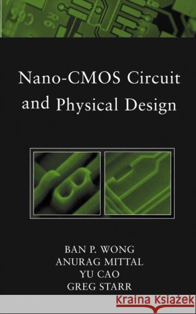
Nano-CMOS Circuit and Physical Design Ban Wong Anurag Mittal Yu Cao 9780471466109 Wiley-Interscience - książkaWidoczna okładka, to zdjęcie poglądowe, a rzeczywista szata graficzna może różnić się od prezentowanej.

Nano-CMOS Circuit and Physical Design

ISBN-13: 9780471466109 / Angielski / Twarda / 2004 / 393 str.

Ban Wong; Anurag Mittal; Yu Cao
cena 799,09 zł
(netto: 761,04 VAT:  5%)

Najniższa cena z 30 dni: 792,54 zł
Termin realizacji zamówienia:
ok. 30 dni roboczych
Bez gwarancji dostawy przed świętami

Darmowa dostawa!

Based on the authors' expansive collection of notes taken over the years, Nano-CMOS Circuit and Physical Design bridges the gap between physical and circuit design and fabrication processing, manufacturability, and yield. This innovative book covers: process technology, including sub-wavelength optical lithography; impact of process scaling on circuit and physical implementation and low power with leaky transistors; and DFM, yield, and the impact of physical implementation.

Kategorie:
Technologie
Kategorie BISAC:
Computers > Computer Engineering
Technology & Engineering > Electronics - Circuits - VLSI & ULSI
Technology & Engineering > Electrical
Wydawca:
Wiley-Interscience
Język:
Angielski
ISBN-13:
9780471466109
Rok wydania:
2004
Ilość stron:
393
Waga:
0.72 kg
Wymiary:
23.16 x 17.58 x 2.54
Oprawa:
Twarda
Wolumenów:
01
Dodatkowe informacje:
Bibliografia
Wydanie ilustrowane

FOREWORD.

PREFACE.

1 NANO–CMOS SCALING PROBLEMS AND IMPLICATIONS.

1.1 Design Methodology in the Nano–CMOS Era.

1.2 Innovations Needed to Continue Performance Scaling.

1.3 Overview of Sub–100–nm Scaling Challenges and Subwavelength Optical Lithography.

1.4 Process Control and Reliability.

1.5 Lithographic Issues and Mask Data Explosion.

1.6 New Breed of Circuit and Physical Design Engineers.

1.7 Modeling Challenges.

1.8 Need for Design Methodology Changes.

1.9 Summary.

References.

PART I: PROCESS TECHNOLOGY AND SUBWAVELENGTH OPTICAL LITHOGRAPHY: PHYSICS, THEORY OF OPERATION, ISSUES, AND SOLUTIONS.

2 CMOS DEVICE AND PROCESS TECHNOLOGY.

2.1 Equipment Requirements for Front–End Processing.

2.2 Front–End–Device Problems in CMOS Scaling.

2.3 Back–End–of–Line Technology.

References.

3 THEORY AND PRACTICALITIES OF SUBWAVELENGTH OPTICAL LITHOGRAPHY.

3.1 Introduction and Simple Imaging Theory.

3.2 Challenges for the 100–nm Node.

3.3 Resolution Enhancement Techniques: Physics.

3.4 Physical Design Style Impact on RET and OPC Complexity.

3.5 The Road Ahead: Future Lithographic Technologies.

References.

PART II: PROCESS SCALING IMPACT ON DESIGN 4 MIXED–SIGNAL CIRCUIT DESIGN.

4.1 Introduction.

4.2 Design Considerations.

4.3 Device Modeling.

4.4 Passive Components.

4.5 Design Methodology.

4.6 Low–Voltage Techniques.

4.7 Design Procedures.

4.8 Electrostatic Discharge Protection.

4.9 Noise Isolation.

4.10 Decoupling.

4.11 Power Busing.

4.12 Integration Problems.

4.13 Summary.

References.

5 ELECTROSTATIC DISCHARGE PROTECTION DESIGN.

5.1 Introduction.

5.2 ESD Standards and Models.

5.3 ESD Protection Design.

5.4 Low–C ESD Protection Design for High–Speed I/O.

5.5 ESD Protection Design for Mixed–Voltage I/O.

5.6 SCR Devices for ESD Protection.

5.7 Summary.

References.

6 INPUT/OUTPUT DESIGN.

6.1 Introduction.

6.2 I/O Standards.

6.3 Signal Transfer.

6.4 ESD Protection.

6.5 I/O Switching Noise.

6.6 Termination.

6.7 Impedance Matching.

6.8 Preemphasis.

6.9 Equalization.

6.10 Conclusion.

References.

7 DRAM.

7.1 Introduction.

7.2 DRAM Basics.

7.3 Scaling the Capacitor.

7.4 Scaling the Array Transistor.

7.5 Scaling the Sense Amplifier.

7.6 Summary.

References.

8 SIGNAL INTEGRITY PROBLEMS IN ON–CHIP INTERCONNECTS.

8.1 Introduction.

8.2 Interconnect Parasitics Extraction.

8.3 Signal Integrity Analysis.

8.4 Design Solutions for Signal Integrity.

8.5 Summary.

References.

9 ULTRALOW POWER CIRCUIT DESIGN.

9.1 Introduction.

9.2 Design–Time Low–Power Techniques.

9.3 Run–Time Low–Power Techniques.

9.4 Technology Innovations for Low–Power Design.

9.5 Perspectives for Future Ultralow–Power Design.

References.

PART III: IMPACT OF PHYSICAL DESIGN ON MANUFACTURING/YIELD AND PERFORMANCE.

10 DESIGN FOR MANUFACTURABILITY.

10.1 Introduction.

10.2 Comparison of Optimal and Suboptimal Layouts.

10.3 Global Route DFM.

10.4 Analog DFM.

10.5 Some Rules of Thumb.

10.6 Summary.

References.

11 DESIGN FOR VARIABILITY.

11.1 Impact of Variations on Future Design.

11.2 Strategies to Mitigate Impact Due to Variations.

11.3 Corner Modeling Methodology for Nano–CMOS Processes.

11.4 New Features of the BSIM4 Model.

11.5 Summary.

References.

INDEX.

BAN P. WONG, IENG MIEE, served for five years as a member of the technical program committee of IEEE International Solid–State Circuits Conference and as session chair, cochair, and organizer of a panel session. He has three issued patents. He has led circuit design teams in developing methodology and implementation of high–performance and low–power microprocessors. He is currently Senior Engineering Manager for NVIDIA Corporation.

ANURAG MITTAL received his PhD in applied physics from Yale University. He has codeveloped novel embedded NVM microcontroller and microprocessor solutions including the world s first truly CMOS–compatible Flash technology. He is Senior Staff Engineer for Virage Logic, Inc.

YU CAO received his PhD in electrical engineering from University of California, Berkeley. He is a postdoctoral researcher in the Berkeley Wireless Research Center. He received the 2000 Beatrice Winner Award at the IEEE International Solid–State Circuits Conference.

GREG STARR received his PhD in electrical engineering from Arizona State University. Currently, he is a Senior Design Manager at Xilinx Corporation.

A practical approach to nano–CMOS circuit design and implementation

The fast pace of new technology and the challenges of nano–scaling are bringing together the once–separate disciplines of circuit design, technology device physics, and physical implementation. A good understanding of the underlying physical constraints of device, interconnect, and manufacturing is crucial for designing circuit systems and devices and making sound technology decisions.

Nano–CMOS Circuit and Physical Design integrates the nanometer process, device manufacturability, advanced circuit design, and related physical implementation into a single, seamless approach to advanced semiconductor technology. This comprehensive volume explores new developments in devices and processing; presents design issues, paying special attention to technology/design interactions such as signal integrity and interconnects; and addresses the impact of design for manufacturability and variability. Important topics include:

  • Nano–CMOS process scaling issues and implications on design
  • Subwavelength optical lithography
  • Physics and theory of operation issues and solutions
  • Design for manufacturability and variability

Written by expert practitioners, Nano–CMOS Circuit and Physical Design is a useful resource for IC designers and professionals in the field, providing them with practical design solutions and approaches.


Udostępnij

Facebook - konto krainaksiazek.pl


Opinie o Krainaksiazek.pl na Opineo.pl

Partner Mybenefit

Krainaksiazek.pl w programie rzetelna firma Krainaksiaze.pl - płatności przez paypal

Czytaj nas na:

Facebook - krainaksiazek.pl
  • książki na zamówienie
  • granty
  • książka na prezent
  • kontakt
  • pomoc
  • opinie
  • regulamin
  • polityka prywatności

Zobacz:

  • Księgarnia czeska

  • Wydawnictwo Książkowe Klimaty

1997-2025 DolnySlask.com Agencja Internetowa

© 1997-2022 krainaksiazek.pl
     
KONTAKT | REGULAMIN | POLITYKA PRYWATNOŚCI | USTAWIENIA PRYWATNOŚCI
Zobacz: Księgarnia Czeska | Wydawnictwo Książkowe Klimaty | Mapa strony | Lista autorów
KrainaKsiazek.PL - Księgarnia Internetowa
Polityka prywatnosci - link
Krainaksiazek.pl - płatnośc Przelewy24
Przechowalnia Przechowalnia