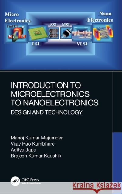
Introduction to Microelectronics to Nanoelectronics: Design and Technology » książka


Introduction to Microelectronics to Nanoelectronics: Design and Technology
ISBN-13: 9780367502379 / Angielski / Twarda / 2020 / 328 str.
Introduction to Microelectronics to Nanoelectronics: Design and Technology
ISBN-13: 9780367502379 / Angielski / Twarda / 2020 / 328 str.
(netto: 580,69 VAT: 5%)
Najniższa cena z 30 dni: 528,93
ok. 16-18 dni roboczych.
Darmowa dostawa!
This book provides thorough analysis and demonstration starting from semiconductor devices to the VLSI fabrication, designing, on-chip interconnect modeling with emerging non-silicon/ nano devices. It gives detailed description of both theoretical as well as industry standard HSPICE, Verilog, Cadence simulation based real-time modeling approaches.
Chapter 1 SEMICONDUCTOR PHYSICS AND DEVICES1.1Introduction 1.1.1Conduction in Solids1.1.2Conductors, Semiconductors, and Insulator1.1.3P-Type and N-Type Semiconductors 1.1.4 Semiconductor Conductivity1.2 Diodes1.2.1Diode Structure and Characteristics1.2.2PN Diode Structure1.2.3Zener Diode Structure1.2.4Diode Applications1.3Bipolar Junction Transistors 1.3.1Symbol and Physical Structure1.3.2BJT Configuration1.3.3Second Order Effects1.4Field Effect Transistors 1.4.1Junction Field Effect Transistors (JFET)1.4.2Metal Oxide Semiconductor Field Effect Transistor (MOSFET)1.4.3Advantages of MOSFET over JFET1.5Emerging Devices beyond MOS1.5.1Issues with CMOS Technology Scaling1.5.2Emerging Nano-scale Device Technologies1.6Summary1.7Multiple Choice Questions1.8Short Answer Questions1.9Long Answer Questions1.10References CHAPTER 2 VLSI SCALING AND FABRICATION2.1Introduction to VLSI Scaling2.1.1History and Introduction of VLSI Technology2.1.2VLSI Design’s Concept2.1.3Moore’s Law2.1.4Scale of Integration2.1.5Types of VLSI Chips ( Analog & Digital)2.1.6Layout, and Micron & Lambda Rules2.2VLSI Fabrication Process2.2.1Purification, Crystal Growth, and Wafer Processing (CZ and FZ Process)2.2.2Oxidation 2.2.3Epitaxial Deposition2.2.4Lithography2.2.5Polysilicon and Dielectric Deposition2.2.6Diffusion2.2.7Ion Implementation 2.2.8Metallization2.2.9Etching Process2.3Basic CMOS Technology2.3.1N-Well and P-Well CMOS Process2.3.2Twin Tub Process2.4Summary2.5Multiple Choice Questions2.6Short Answer Questions2.7Long Answer Questions2.8References CHAPTER 3 MOSFET MODELING 3.1Introduction to MOS Transistor 3.1.1Characteristics of MOS Transistor3.1.2Hot Carrier Effects3.1.3Parasitics of MOSFET3.1.4MOSFET Circuit Models3.2MOS Capacitor3.2.1MOS Capacitor with Zero and Nonzero Bias3.2.2Capacitance-Voltage Curves3.2.3Anomalous Capacitance-Voltage Curves3.3MOSFET DC and Dynamic Models3.3.1Pao-Sah Model3.3.2Charge Sheet Model3.3.3Piece-Wise Model for Enhancement Devices3.3.4Small Geometry Model3.3.5Intrinsic Charge and Capacitance3.3.6Meyer Model3.4MOSFET Modeling using SPICE3.4.1Basic Concepts of Modeling3.4.2Model Equations3.4.3Examples using HSPICE3.5Summary3.6Multiple Choice Questions3.7Short Answer Questions3.8Long Answer Questions3.9References CHAPTER 4 COMBINATIONAL AND SEQUENTIAL DESIGN IN CMOS4.1CMOS Inverter 4.1.1Design 4.1.2Operation4.1.3Transient and VTC Characteritsitics 4.1.4Significance of CMOS Inverter4.2 Static Behavior of Inverter4.2.1Switching Threshold4.2.2Noise Margin4.2.3Robustness of CMOS inverter by scaling supply voltage4.3Dynamic behavior of CMOS inverter4.3.1Capacitances4.3.2Power and Energy consumption4.4Design of Combinational Logic Design 4.4.1Complementary CMOS logic4.4.2Ratioed Logic4.4.3Pass-Transistor Logi4.5CMOS Sequential Design4.5.1Introduction4.5.2Metrics for CMOS Sequential Design4.6Static Latches and Registers 4.6.1The Bistability Principle4.6.2SR Flip-Flops4.6.3D-latches and Flip-Flops4.6.4Master slave Flip-flop4.7Summary4.8Multiple Choice Questions4.9Short Questions4.10Long Questions4.11References CHAPTER 5 ANALOG CIRCUIT DESIGN5.1Introduction to Analog Design5.2MOS device from Analog perspective5.2.1I/V Characteristics 5.2.2Second-order Effects5.2.3MOS Small Signal Model 5.3Single Stage Amplifier 5.3.1Common Source5.3.2Common Gate5.3.3Source Follower5.4Current mirrors5.4.1Introduction5.4.2Basic Current Mirror5.4.3Cascode current Mirror5.5Differential Amplifiers5.5.1Single ended and differential Operation5.5.2Basic Differential Pair5.5.3Differential Pair with MOS load5.6Operational Amplifiers5.6.1Fundamentals and General Op-amp metrics5.6.2Two Stage Op-amp5.7Digital-to-Analog and Analog-to-Digital Converters5.7.1Introduction 5.7.2Types of Digital-to-Analog Converters5.7.3Types of Analog-to-Digital Converters5.8Summary5.9Multiple Choice Questions5.10Short Answer Questions5.11Long Answer Questions5.12ReferencesCHAPTER 6: DIGITAL DESIGN THROUGH VERILOG HDL6.1Introduction 6.1.1What is Verilog HDL6.1.2Backgrounnd6.1.3Compiler Directives6.1.4Data Types6.1.5Operators6.2Module and Test bench Definitions6.2.1Module6.2.2Test bench6.3Gate-Level Modeling 6.3.1Built-in primitives 6.3.2Single and multiple input gates6.3.3Tristate gates6.3.4MOS Switch6.3.5Gate Delays 6.3.6Example6.4 Dataflow Modeling6.4.1Continuous Assignments6.4.2Delays6.4.3Examples: Verilog Program for Full Adder6.5 Behavioral Modeling6.5.1Initial Statement6.5.2Always Statement6.5.3Procedural Assignments6.5.4Conditional Statements 6.5.5Loop Statements6.5.6Examples6.6 Tasks and Functions6.6.1Tasks6.6.2Functions6.7Summary6.8Multiple Choice Questions6.9Short Questions6.10Long Questions6.11References CHAPTER 7 VLSI INTERCONNECT AND IMPLEMENTATION7.1An overview of the VLSI Interconnect Problem7.1.1Interconnect Scaling Problem7.1.2Implementation of Interconnect Problem7.2Interconnect Aware Design Methodology and Electrical Modeling7.2.1Impact of Scaling7.2.2Transistor Scaling7.2.3Interconnect Scaling7.3Electrical Circuit Model of Interconnect7.3.1Ideal Interconnect7.3.2Resistive Interconnect7.3.3Capacitive Interconnect7.3.4Resistive Interconnect Tree7.4Estimation of Interconnect Parasitics7.4.1Interconnect Resistance Estimation7.4.2Interconnect Inductance Estimation7.4.3Interconnect Capacitance Estimation7.4.3.1Parallel Plate Capacitor7.4.3.2Fringing Capacitance7.4.3.3Lateral Capacitance7.5Calculation of Interconnect Delay7.5.1RC Delay Model7.5.2Elmore Delay Model7.5.3Transfer Function Model based on ABCD Parameter matrix7.5.4Finite Difference Time Domain Model (FDTD)7.6Estimation of Interconnect Crosstalk Noise7.7Estimation of Interconnect Power Dissipation7.8Summary7.9Multiple Choice Questions7.10Short Answer Questions7.11Long Answer Questions7.12References CHAPTER 8 VLSI DESIGN AND TESTABILITY 8.1Preamble8.2Basic Digital Troubleshoot 8.2.1Manufacturing Test8.2.2Tester and Test Fixtures8.2.3Test Programs8.3Effect of Physical Faults on Circuit Behavior8.3.1Fault Models8.3.1.1Line Stuck-at Faults8.3.1.2Transistor Stuck-at Faults8.3.1.3Floating Line Faults8.3.1.4Bridging Faults8.4Test Principles of Manufacturing8.4.1Observability8.4.2Controllability8.4.3Fault Coverage8.4.4Automatic Test Pattern Generation (ATPG)8.4.5Delay Fault Testing 8.5Test Approaches8.5.1Ad Hoc DFT Techniques8.5.2Scan Design Test8.5.3Built-in-Self-Test (BIST)8.5.4IDDQ Testing8.6 Design for Manufacturability (DFM)8.7 System on Chip (SOC) Testing8.8 Summary8.9Multiple Choice Questions8.10Short Answer Questions8.11Long Questions8.12References CHAPTER 9 NANO-MATERIALS AND APPLICATIONS9.1Preamble of Nano-Materials9.2Introduction to Carbon Nanotubes (CNTs)9.2.1The concept of Chirality on CNT9.2.2Electronic Band Structure9.2.3Brillouin zone9.3Overview of Graphene Nanoribbon (GNR)9.4Properties of CNT and GNR9.5Fabrication Approaches for Graphene Nanostructure9.5.1The transfer process of graphene on the Si/SiO2 substrate9.5.2CNT Fabrications9.6Application of Nano-materials9.6.1Graphene Nanoribbon Interconnect9.6.2Carbon Nanotube based Interconnect9.6.3Nano-Sensor9.6.4Nanomaterial Based Combat Jacket 9.6.5Nano Bio-Sensor for Drug Delivery9.7 Summary9.8Multiple Choice Questions9.9Short Answer Questions9.10Long Answer Questions9.11References CHAPTER 10 NANOSCALE TRANSISTORS10.1Issues with CMOS technology scaling10.1.1Velocity Saturation and Mobility Degradation 10.1.2Tunneling Limit10.1.3High Field Effects10.1.4Power Limitation10.1.5Material limitation 10.2Tunnel FET10.2.1Device Structure and Models10.2.2Device Characteristics10.2.3TFET based Circuit design 10.3Negative Capacitance FET10.3.1Device Structure 10.3.2Principle of operation10.3.3Low subthreshold swing and high ON current10.3.4Hysteresis Characteristics10.3.5NCFET device based inverter and digital logic design10.4Carbon Nanotube FET10.4.1Carbon nanotube (CNT) 10.4.2 Carbon nanotube FET (CNTFET)10.4.2Device Characteristics10.5Graphene Nanoribbon FET10.5.1Graphene structure and properties10.5.2Graphene nanoribbon FET (GNRFET)10.6Spintronic Devices 10.6.1Principle of Operation10.6.2Spin based Devices10.7Summary10.8Multiple Choice Questions10.9Short Answer Questions10.10Long Answer Questions10.11References MCQ ANSWERS
1997-2026 DolnySlask.com Agencja Internetowa
KrainaKsiazek.PL - Księgarnia Internetowa


