Embedded and Fan-Out Wafer and Panel Level Packaging Technologies for Advanced Application Spaces: High Performance Compute and System-In-Package » książka


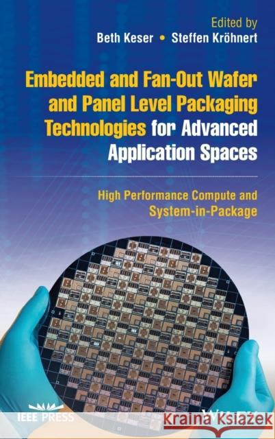
Embedded and Fan-Out Wafer and Panel Level Packaging Technologies for Advanced Application Spaces: High Performance Compute and System-In-Package
ISBN-13: 9781119793779 / Angielski / Twarda / 2021 / 320 str.
Embedded and Fan-Out Wafer and Panel Level Packaging Technologies for Advanced Application Spaces: High Performance Compute and System-In-Package
ISBN-13: 9781119793779 / Angielski / Twarda / 2021 / 320 str.
(netto: 587,39 VAT: 5%)
Najniższa cena z 30 dni: 600,66
ok. 30 dni roboczych.
Darmowa dostawa!
Preface xv1 Fan-Out Wafer and Panel Level Packaging Market and Technology Trends 1Santosh Kumar, Favier Shoo, and Stephane Elisabeth1.1 Introduction to Fan-Out Packaging 11.1.1 Historical Perspective 11.1.2 Key Drivers: Why Fan-Out Packaging? 61.1.3 FO-WLP vs. FO-PLP 81.1.4 Future of Fan-Out Packaging for Heterogeneous Integration 81.2 Market Overview and Applications 101.2.1 Fan-Out Packaging Definition 101.2.2 Market Segmentation: Core FO vs. HD FO vs. UHD FO 111.2.3 Market Valuation: Forecast of Revenue and Volume 121.2.4 Current and Future Target Markets 121.2.5 Applications of Fan-Out Packaging 141.3 Technology Trends and Supply Chain 191.3.1 Fan-Out Packaging Technology Roadmaps 191.3.2 Fan-Out Packaging Technology by Manufacturer 191.3.2.1 Amkor 191.3.2.2 JCET 201.3.2.3 NXP 211.3.2.4 DECA Technologies 211.3.2.5 ASE 221.3.2.6 TSMC 221.3.2.7 PTI 241.3.2.8 Samsung Electronics 251.3.2.9 Huatian 251.3.3 Supply Chain Overview 251.3.4 Analysis of the Latest Developments in the Supply Chain 261.4 Fan-Out Panel-Level Packaging (FO-PLP) 291.4.1 Motivation and Challenges for FO-PLP 291.4.2 FO-PLP Market and Applications 301.4.3 FO-PLP Supplier Overview 311.5 SystemDevice Teardowns 341.5.1 Teardown of End-Systems with Fan-Out Packaging 341.5.2 Technology Comparison 381.5.2.1 Radar IC: eWLB vs. RCP 381.5.2.2 MCM/SiP: RCP-SiP vs. eWLB 391.5.2.3 PMIC: eWLB vs. M-Series 401.5.3 Cost Comparison 411.6 Conclusion 42References 452 Cost Comparison of FO-WLP with Other Technologies 47Amy Palesko Lujan2.1 Introduction 472.2 Activity-Based Cost Modeling 472.3 Cost Analysis of FO-WLP Variations 492.3.1 Process Segment Costs 502.3.1.1 Die Preparation 502.3.1.2 Carrier 502.3.1.3 Die Bond 512.3.1.4 Mold 512.3.1.5 Backgrinding 512.3.1.6 RDL 512.3.1.7 UBM 522.3.1.8 Flux and Ball Attach 522.3.1.9 Singulation 522.3.2 FO-WLP Variations 522.3.2.1 Carrier 542.3.2.2 Die Cost and Preparation 542.3.2.3 Die Bond 542.3.2.4 Mold/Mold+CUF 542.3.2.5 Backgrind/Post-mold Grind 542.3.2.6 Scrap 552.4 Cost of FO-WLP versus Wire Bond and Flip Chip 552.5 Package-on-Package Cost Analysis 612.5.1.1 Substrate/RDLs 632.5.1.2 Die Bond 632.5.1.3 CUF and Mold Cost 632.5.1.4 Ball Attach 642.5.1.5 Singulation 642.5.1.6 TMV 642.5.1.7 Die Bond 662.5.1.8 CUF and Mold Cost 662.5.1.9 TMV/Large Copper Pillars 662.6 Conclusions 66References 673 Integrated Fan-Out (InFO) for Mobile Computing 69Doug C.H. Yu, John Yeh, Kuo-Chung Yee, and Chih Hang Tung3.1 Introduction 693.2 Fan-InWafer-Level Packaging 703.2.1 Dielectric and Redistribution Layers (RDL) 713.2.2 Under Bump Metallization (UBM) 713.2.3 Reliability and Challenges 723.2.4 Large Die WLP 723.3 Fan-OutWafer-Level System Integration 733.3.1 Chip-First vs. Chip-Last 743.3.2 Molding and Planarization 753.3.3 Redistribution Layer (RDL) 773.3.4 Through Via and Vertical Interconnection 803.4 Integrated Passive Devices (IPDs) 813.4.1 High Q-Factor 3D Solenoid Inductor 813.4.2 Antenna in Package (AiP) and 5G Communication 813.4.3 Passive Devices for MillimeterWave System Integration 823.5 Power, Performance, Form Factor, and Cost 853.5.1 Signal and Power Integrity 873.5.2 Heat Dissipation and Thermal Performance 883.5.3 Form Factor and Thickness 913.5.4 Cycle Time to Market and Cost 913.6 Summary 91References 924 Integrated Fan-Out (InFO) for High Performance Computing 95Doug C.H. Yu, John Yeh, Kuo-Chung Yee, and Chih Hang Tung4.1 Introduction 954.2 3DFabric and System-on-Integrated-Chip (SoIC) 974.3 CoWoS-R, CoWoS-S, and CoWoS-L 994.4 InFO-L and InFO-R 1004.5 Info Ultra-High-Density Interconnect (InFO-UHD) 1004.6 Multi-Stack System Integration (MUST) and Must-in-Must (MiM) 1064.7 InFO on Substate (InFO-oS) and InFO Local Silicon Interconnect (InFO-L) 1084.8 InFO with Memory on Substrate (InFO-MS) 1104.9 InFO 3D Multi-Silicon (InFO-3DMS) and CoWoS-L 1114.10 InFO System onWafer (InFO_SoW) 1124.11 System on Integrated Substrate (SoIS) 1164.12 Immersion Memory Compute (ImMC) 1164.13 Summary 121References 1225 Adaptive Patterning and M-Series for High Density Integration 125Benedict San Jose, Cliff Sandstrom, Jan Kellar, Craig Bishop, and Tim Olson5.1 Technology Description 1255.2 Applications and Markets 1275.3 Basic Package Construction 1275.4 Manufacturing Process Flow and BOM 1315.5 Design Features and System Integration Capability 1345.6 Adaptive Patterning 1375.7 Manufacturing Format and Scalability 1445.8 Package Performance 1495.9 Robustness and Reliability Data 1515.10 Electrical Test Considerations 1525.11 Summary 153References 1536 Panel-Level Packaging for Heterogenous Integration 155M. Töpper, T. Braun, M. Billaud, and L. Stobbe6.1 Introduction 1556.2 Fan-Out Panel-Level Packaging 1576.3 Economic Efficiency Analysis of PLP 1616.4 Summary 165References 1667 Next Generation Chip Embedding Technology for High Efficiency Power Modules and Power SiPs 169Vikas Gupta, Kay Essig, C.T. Chiu, and Mark Gerber7.1 Technology Description 1697.2 Basic Package Construction 1727.3 Applications and Markets (HPC, SiP) 1767.4 Manufacturing Process Flow and BOM 1777.5 Design Features 1807.6 System Integration Capability 1827.7 Package Performance 1837.8 Robustness and Reliability Data 1867.9 Electrical Test Considerations 1907.10 Summary 191References 1928 Die Integration Technologies on Advanced Substrates Including Embedding and Cavities 193Markus Leitgeb and Christian Vockenberger8.1 Introduction 1938.2 Heterogeneous Integration by Use of Embedded Chip Packaging (ECP(r)) 1948.3 Embedding Process 1968.4 Component Selection 1988.5 Design Technology 1998.6 Testing 2008.7 Applications for ECP Technology 2018.8 Heterogeneous Integration Using Cavities in PCB 2068.9 Package Performance, Robustness, and Reliability 2088.10 Conclusion 215References 2159 Advanced Embedded Trace Substrate - A Flexible Alternative to Fan-Out Wafer Level Packaging 217Shih Ping Hsu, Byron Hsu, and Adan Chou9.1 Technology Description 2179.1.1 C²iM Technology 2179.1.2 C²iM-PLP Technology 2189.2 Applications and Markets 2199.3 Basic Package Construction 2199.3.1 C²iM-PLP Experience 2199.3.2 C²iM-PLP Advantages and Disadvantages Compared to Wirebond Quad Flat No Lead (WB-QFN) and Flip-Chip QFN (FC-QFN) Packages 2199.3.3 C²iM-PLP Advantages and Disadvantages Compared to WLP and FO-WLP 2209.3.4 Future Applications 2229.3.5 Limitations of C²iM-PLP 2229.4 Manufacturing Process Flow and BOM 2239.5 Design Features 2249.5.1 Package Design Rules 2249.5.2 Design Rules for Die UBM 2249.5.3 Design Rules for Die Side by Side 2259.5.4 Design Rules for Cu Pillar 2269.6 System Integration Capability 2279.7 Manufacturing Format and Scalability 2289.8 Package Performance 2289.8.1 Electrical Performance 2289.8.2 Thermal Performance 2299.9 Robustness and Reliability Data 2299.9.1 Automotive Reliability Certification Pass 2299.9.2 Board Level Reliability Verification Pass 2309.10 Electrical Test Considerations 2309.11 Summary 231References 23110 Flexible Hybrid Electronics Using Fan-Out Wafer-Level Packaging 233Subramanian S. Iyer and Arsalan Alam10.1 Introduction 23310.2 Recent Trends in Packaging 23910.3 FHE Using FO-WLP - FlexTrate(TM) 24210.4 Applications on FlexTrate(TM) 250Acknowledgments 256References 25611 Polylithic Integrated Circuits using 2.5D and 3D Heterogeneous Integration: Electrical and Thermal Design Considerations and Demonstrations 261Ting Zheng, Ankit Kaul, Sreejith Kochupurackal Rajan, and Muhannad S. Bakir11.1 Introduction 26111.2 Heterogeneous Interconnect Stitching Technology (HIST) 26211.3 Thermal Evaluation of 2.5D Integration Using Bridge-Chip Technology 27011.3.1 2.5D and 3D Benchmark Architectures 27011.3.1.1 2.5D Integration 27011.3.1.2 3D Integration 27111.3.2 Thermal Modeling and Specifications 27211.3.3 Comparison of Different 2.5D Integration Schemes 27311.3.4 Thermal Comparison between 2.5D and 3D Integration 27311.3.5 Thermal Study of Bridge-Chip 2.5D Integration 27411.3.5.1 Impact of TIM conductivity 27411.3.5.2 Die Thickness 27511.3.5.3 Die Spacing 27511.3.6 Polylithic 3D Integration 27511.4 Monolithic Microfluidic Cooling of High-Power Electronics 27611.4.1 Experimental Demonstration and Characterization on Single Die Systems 27711.4.2 Microfluidic Cooling of 2.5D Devices: Experimental Demonstration 27911.4.3 Monolithic Microfluidic Cooling of 3D Integration: Modelling Electrical Implications for I/Os 28111.5 Conclusion 283Acknowledgments 283References 283Index 289
Beth Keser, PhD, is an IEEE Fellow and Distinguished Lecturer with over 23 years' experience in the semiconductor industry and a co-Editor of Advances in Embedded and Fan-Out Wafer Level Packaging Technologies. Beth's excellence in developing revolutionary electronic packages for semiconductor devices has resulted in 30 patents and patents pending and over 50 publications in the semiconductor industry.Steffen Kröhnert is President & Founder of ESPAT-Consulting in Dresden, Germany. He is member of IEE EPS and co-Editor of Advances in Embedded and Fan-Out Wafer Level Packaging Technologies. Steffen has over 20 years' experience in the semiconductor industry and is the author or co-author of 23 patent filings.
1997-2026 DolnySlask.com Agencja Internetowa
KrainaKsiazek.PL - Księgarnia Internetowa


