• Wyszukiwanie zaawansowane
  • Kategorie
  • Kategorie BISAC
  • Książki na zamówienie
  • Promocje
  • Granty
  • Książka na prezent
  • Opinie
  • Pomoc
  • Załóż konto
  • Zaloguj się

75th Anniversary of the Transistor » książka

zaloguj się | załóż konto
Logo Krainaksiazek.pl

koszyk

konto

szukaj
topmenu
Księgarnia internetowa
Szukaj
Książki na zamówienie
Promocje
Granty
Książka na prezent
Moje konto
Pomoc
 
 
Wyszukiwanie zaawansowane
Pusty koszyk
Bezpłatna dostawa dla zamówień powyżej 20 złBezpłatna dostawa dla zamówień powyżej 20 zł

Kategorie główne

• Nauka
 [2949965]
• Literatura piękna
 [1857847]

  więcej...
• Turystyka
 [70818]
• Informatyka
 [151303]
• Komiksy
 [35733]
• Encyklopedie
 [23180]
• Dziecięca
 [617748]
• Hobby
 [139972]
• AudioBooki
 [1650]
• Literatura faktu
 [228361]
• Muzyka CD
 [398]
• Słowniki
 [2862]
• Inne
 [444732]
• Kalendarze
 [1620]
• Podręczniki
 [167233]
• Poradniki
 [482388]
• Religia
 [509867]
• Czasopisma
 [533]
• Sport
 [61361]
• Sztuka
 [243125]
• CD, DVD, Video
 [3451]
• Technologie
 [219309]
• Zdrowie
 [101347]
• Książkowe Klimaty
 [123]
• Zabawki
 [2362]
• Puzzle, gry
 [3791]
• Literatura w języku ukraińskim
 [253]
• Art. papiernicze i szkolne
 [7933]
Kategorie szczegółowe BISAC

75th Anniversary of the Transistor

ISBN-13: 9781394202447 / Angielski

Arockia Nathan; Samar Saha; Ravi M. Todi
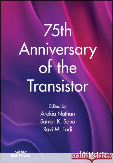
75th Anniversary of the Transistor Arockia Nathan Samar Saha Ravi M. Todi 9781394202447 Wiley-IEEE Press - książkaWidoczna okładka, to zdjęcie poglądowe, a rzeczywista szata graficzna może różnić się od prezentowanej.

75th Anniversary of the Transistor

ISBN-13: 9781394202447 / Angielski

Arockia Nathan; Samar Saha; Ravi M. Todi
cena 407,30 zł
(netto: 387,90 VAT:  5%)

Najniższa cena z 30 dni: 403,13 zł
Termin realizacji zamówienia:
ok. 30 dni roboczych
Bez gwarancji dostawy przed świętami

Darmowa dostawa!

75th Anniversary of the Transistor 75th anniversary commemorative volume reflecting the transistor's development since inception to current state of the art 75th Anniversary of the Transistor is a commemorative anniversary volume to celebrate the invention of the transistor. The anniversary volume was conceived by the IEEE Electron Devices Society (EDS) to provide comprehensive yet compact coverage of the historical perspectives underlying the invention of the transistor and its subsequent evolution into a multitude of integration and manufacturing technologies and applications. The book reflects the transistor's development since inception to the current state of the art that continues to enable scaling to very large-scale integrated circuits of higher functionality and speed. The stages in this evolution covered are in chronological order to reflect historical developments. Narratives and experiences are provided by a select number of venerated industry and academic leaders, and retired veterans, of the semiconductor industry. 75th Anniversary of the Transistor highlights: Historical perspectives of the state-of-the-art pre-solid-state-transistor world (pre-1947) leading to the invention of the transistor Invention of the bipolar junction transistor (BJT) and analytical formulations by Shockley (1948) and their impact on the semiconductor industry Large scale integration, Moore's Law (1965) and transistor scaling (1974), and MOS/LSI, including flash memories — SRAMs, DRAMs (1963), and the Toshiba NAND flash memory (1989) Image sensors (1986), including charge-coupled devices, and related microsensor applications With comprehensive yet succinct and accessible coverage of one of the cornerstones of modern technology, 75th Anniversary of the Transistor is an essential reference for engineers, researchers, and undergraduate students looking for historical perspective from leaders in the field.

Kategorie:
Technologie
Kategorie BISAC:
Technology & Engineering > Electronics - Semiconductors
Technology & Engineering > Electronics - Transistors
Wydawca:
Wiley-IEEE Press
Język:
Angielski
ISBN-13:
9781394202447

Editor Biography xiiiPreface xv1 The First Quantum Electron Device 1Leo Esaki2 IEEE Electron Devices Society: A Brief History 3Samar K. Saha2.1 Introduction 32.2 Origins of EDS 42.3 Growth of EDS 62.4 Publications 102.5 Conferences 122.6 Awards and Recognition 142.7 Conclusion 143 Did Sir J.C. Bose Anticipate the Existence of p- and n-Type Semiconductors in His Coherer/Detector Experiments? 17Prasanta Kumar Basu3.1 Introduction 173.2 J.C. Bose: A Brief Biography 183.3 Bose's Work on Detectors 193.4 Mott's Remark 213.5 Understanding Semiconductors and Doping 213.6 Interpretation of Mott's Remark 233.7 Conclusion 254 The Point-Contact Transistor: A Revolution Begins 29John M. Dallesasse and Robert B. Kaufman4.1 Introduction 294.2 Background and Motivation 304.3 Inventors' Understanding How a Point-Contact Transistor Operates 314.4 Recreating the Point-Contact Transistor 334.5 Concluding Remarks 405 On the Shockley Diode Equation and Analytic Models for Modern Bipolar Transistors 43T. H. Ning5.1 Introduction 435.2 Adaptation of Shockley Diode Equation to Modern Bipolar Transistors 455.3 Modern Bipolar Transistors Structures 465.4 Analytic Models for Modern Bipolar Transistors 485.5 Discussion 496 Junction-Less Field Effect Transistors: The First Transistor to be Conceptualized 51Mamidala Jagadesh Kumar and Shubham Sahay6.1 Introduction 516.2 Structure and Operation 526.3 Salient Features of JLFETs 556.4 Challenges for JLFETs 586.5 Unconventional Applications of JL Architecture 596.6 Conclusions 617 The First MOSFET Design by J. Lilienfeld and a Long Journey to Its Implementation 65Hiroshi Iwai7.1 Introduction 657.2 Demand for the Development of the Solid-State Amplifier and Its Difficulty 667.3 Grid-Inserted MESFETs 687.4 Lilienfeld Patents for the MESFET and MOSFET 697.5 Necessary Conditions for Successful MOSFET Operation, and MOSFET Development Chronology 727.6 Status of the Semiconductor Physics at the Lilienfeld Period (in the 1920s) and Thereafter 737.7 Improvement of Si and Ge Material Quality and Discovery of the pn Junction in the 1940s 747.8 H. Welker's MISFET with Inversion Channel in 1945 757.9 Shockley's Group Study for MOSFET from 1945 to 1947 767.10 Technology Development in the 1950s Until the Successful MOSFET Operation in 1960 797.11 Success of MOSFET Operation by D. Kahng and M. Attala in 1960 817.12 After the First Successful Operation of the MOSFET 827.13 Summary and Conclusions 828 The Invention of the Self-Aligned Silicon Gate Process 89Robert E. Kerwin9 The Application of Ion Implantation to Device Fabrication: The Early Days 95Alfred U. MacRae9.1 Introduction 959.2 Device Fabrication 969.3 Summary 9910 Evolution of the MOSFET: From Microns to Nanometers 101Yuan Taur10.1 Introduction 10110.2 The Early Days: Before 1980 10210.3 From 1980 to 2000 10310.4 The Latest: After 2000 10910.5 Conclusion 11311 The SOI Transistor 115Sorin Cristoloveanu11.1 The Beginnings 11511.2 The Renaissance 11611.3 The Smart-Cut Dynasty 11911.4 Special Mechanisms in FD-SOI MOSFET 12211.5 A Selection of Innovating Devices 12611.6 The Future 13012 FinFET: The 3D Thin-Body Transistor 135Chenming Hu12.1 The Show Stopper 13512.2 The Cause of the Power Crises 13512.3 The Real Cause of the Power Crises 13712.4 A DARPA Request for Proposal 13812.5 The Challenges and Team Work 13912.6 Further Advancements by Industry 14112.7 Conclusion 14413 Historical Perspective of the Development of the FinFET and Process Architecture 145Digh Hisamoto13.1 Introduction 14513.2 Requirements for the End of CMOS Scaling 14613.3 Restrictions of Planar Process Technology 14813.4 Prompted Device/Process Technology Evolution by FinFET 15113.5 Conclusion 15214 The Origin of the Tunnel FET 155Gehan A. J. Amaratunga14.1 Background 15514.2 Conception 15614.3 Realization 15714.4 Relevance 15914.5 Prospects 15915 Floating-Gate Memory: A Prime Technology Driver of the Digital Age 163S. M. Sze15.1 Introduction 16315.2 The Charge-Storage Concept 16415.3 Early Device Structures 16715.4 Multi-Level Cells and 3D Structures 16915.5 Applications 17115.6 Scaling Challenges 17315.7 Alternative Structures 17415.8 Conclusion 17516 Development of ETOX NOR Flash Memory 179Stefan K. Lai16.1 Introduction 17916.2 Background 17916.3 Not the Perfect Solution 18116.4 ETOX Development Challenges 18216.5 Building a Business 18316.6 Closing Words 18417 History of MOS Memory Evolution on DRAM and SRAM 187Mitsumasa Koyanagi17.1 Introduction 18717.2 Revolutionary Technologies in DRAM History 18717.3 Revolutionary Technologies in SRAM History 20217.4 Summary 21018 Silicon-Germanium Heterojunction Bipolar Transistors: A Retrospective 215Subramanian S. Iyer and John D. Cressler18.1 Introduction (JDC) 21518.2 Some History from Early Days at IBM Research (SSI) 21818.3 SiGe Epitaxy and Making the First SiGe Transistor (SSI) 22118.4 MBE vs. UHV/CVD vs. APCVD for SiGe epi (SSI) 22418.5 Putting Physics to Work - The Properties of SiGe HBTs (JDC) 22518.6 SiGe BiCMOS: Devices to Circuits to Systems (JDC and SSI) 22818.7 Using SiGe in Extreme Environments (JDC) 23118.8 New Directions (JDC and SSI) 23418.9 Some Parting Words (SSI) 23519 The 25-Year Disruptive Path of InP/GaAsSb Double Heterojunction Bipolar Transistors 239Colombo R. Bolognesi19.1 Introduction 23919.2 Phase I: Simon Fraser Years (1995-2006) 24219.3 Phase II: ETH Years (2006-2022) 24619.4 Response to Innovation 24819.5 Final Words 24920 The High Electron Mobility Transistor: 40 Years of Excitement and Surprises 253Jesús A. del Alamo20.1 Introduction 25320.2 HEMT Electronics 25420.3 Modulation-Doped Structures in Physics 25720.4 Exciting Prospects 25820.5 Conclusions 25921 The Thin Film Transistor and Emergence of Large Area, Flexible Electronics and Beyond 263Yue Kuo, Jin Jang, and Arokia Nathan21.1 Birth of Large Area Electronics 26321.2 Polycrystalline Silicon and Oxide Thin Film Transistor 26521.3 Trends in TFT Development 26622 Imaging Inventions: Charge-Coupled Devices 273Michael F. Tompsett22.1 Setting the Stage for the Invention of the Charge-Coupled Device (CCD) 27322.2 The Invention of the CCD 27422.3 Verifying the CCD Concept 27522.4 The Invention of CCD Imagers 27622.5 The First Solid-State Color TV Camera 27622.6 Mixed Analog Design Modem Chip 27823 The Invention and Development of CMOS Image Sensors: A Camera in Every Pocket 281Eric R. Fossum23.1 Introduction 28123.2 Underlying Technology 28223.3 Early Solid-State Image Sensors 28323.4 Invention of CMOS Image Sensors 28523.5 Photon-Counting CMOS Image Sensors 28823.6 Conclusion 29024 From Transistors to Microsensors: A Memoir 293Henry Baltes24.1 Early Encounters 29324.2 Integration 29324.3 Silicon Sensors 29424.4 Transistor Sensors 29424.5 CMOS End Fabrication 29624.6 Outlook 29725 Creation of the Insulated Gate Bipolar Transistor 299B. Jayant Baliga25.1 Introduction 29925.2 Historical Context 30025.3 The Brock Effect 30125.4 My IGBT Proposal 30125.5 The Welch Edict 30125.6 Manufacturing the First IGBT Product 30225.7 First IGBT Product Release 30325.8 IGBT Technology Enhancement 30425.9 IGBT Evolution 30525.10 IGBT Applications 30625.11 IGBT Social Impact 30625.12 My Sentiments 30726 The History of Noise in Metal-Oxide-Semiconductor Field-Effect Transistors 309Renuka P. Jindal26.1 Introduction 30926.2 MOSFET Noise Time Line 31026.3 Channel Thermal Noise 31126.4 Induced Gate and Substrate Current Noise 31126.5 Gate-Drain Current Noise Cross Correlation 31226.6 Equilibrium Noise 31226.7 Bulk Charge Effects 31226.8 Gate Resistance Noise 31326.9 Substrate Resistance Noise 31326.10 Substrate and Gate Current Noise 31326.11 Short-Channel Effects 31426.12 Effect on Channel Thermal Noise 31526.13 1/f Noise 31626.14 Conclusions 31627 A Miraculously Reliable Transistor: A Short History 323Muhammad Ashraful Alam and Ahmed Ehteshamul Islam27.1 Introduction: A Transistor is Born 32327.2 Transistor Reliability in the Proto-Scaling Era 32527.3 Reliability of Geometric-and Equivalent-Scaling Eras 32527.4 Conclusions: Reliability Challenges for the Hyper-Scaling and Functional-Scaling Eras 33028 Technology Computer-Aided Design: A Key Component of Microelectronics' Development 337Siegfried Selberherr and Viktor Sverdlov28.1 Introduction 33728.2 Short History 33828.3 Scaling and Model Complexity 33928.4 MINIMOS Commercialization and Beyond 34228.5 Design Technology Co-Optimization at Advanced Nodes 34328.6 Electron Spin for Microelectronics 34328.7 Summary and Outlook 34429 Early Integrated Circuits 349Willy Sansen30 A Path to the One-Chip Mixed-Signal SoC for Digital Video Systems 355Akira Matsuzawa30.1 Introduction 35530.2 Bipolar ADCs at Early Development Stage of Digital TVs 35630.3 A CMOS ADC for Digital Handy Camcorder 36030.4 One-Chip Mixed-Signal SoC for DVD 36331 Historical Perspective of the Nonvolatile Memory and Emerging Computing Paradigms 369Ming Liu31.1 Introduction 36931.2 Rise of Solid-State Nonvolatile Memory 37031.3 NVM in Classical Computer Architectures 37331.4 NVM-Driven New Computing Paradigm 37531.5 Conclusion 37632 CMOS Enabling Quantum Computing 379Edoardo Charbon32.1 Why Cryogenic Electronics? 37932.2 The Quantum Stack 38032.3 Modeling Cryo-CMOS Devices 38032.4 Specific Effects in Cryo-CMOS Transistors 38332.5 Perspectives and Trends 38333 Materials and Interfaces: How They Contributed to Transistor Development 387Bruce Gnade33.1 Introduction 38733.2 Back-End-of-Line 38833.3 Channel Materials 38933.4 Gate Stack 39033.5 Contacts 39133.6 Summary 39134 The Magic of MOSFET Manufacturing 393Kelin J. Kuhn34.1 Introduction 39334.2 The Magic of MOS 39434.3 The Magic of Self-alignment 39734.4 The Magic of Semiconductor Manufacturing 39834.5 Transistor Magic for the NEXT 75 Years? 40035 Materials Innovation: Key to Past and Future Transistor Scaling 403Tsu-Jae King Liu and Lars P. Tatum35.1 Introduction 40335.2 MOSFET Basics 40435.3 Complementary MOS (CMOS) Technology 40735.4 MOSFET Scaling Challenges 40835.5 MOSFET Materials Innovations 41035.6 Outlook for Continued Transistor Scaling 41136 Germanium: Back to the Future 415Krishna C. Saraswat36.1 Introduction 41536.2 Need for High Mobility Material for MOS Channel 41736.3 Surface Passivation of Ge-Based MOSFETs 41836.4 Low Resistance Contacts to Ge 42036.5 Heteroepitaxial Growth of Ge on Si 42236.6 Strained Ge and Heterostructure FETs 42336.7 Nanoscale Ge FETs 42536.8 Ge NMOSFETs 42536.9 Ge-Based Novel Devices for Optical Interconnects 42636.10 Summary 427Acknowledgment 427References 428Index 431

Arokia Nathan, PhD, formerly the Professor of Photonic Systems and Displays at the University of Cambridge, is currently a Bye Fellow and Graduate Tutor at Darwin College, Cambridge.Samar K. Saha, PhD, is an internationally recognized expert on IC device architecture, process and device simulation, and device modeling within the industry and academia.Ravi M. Todi, PhD, is well known in the semiconductor industry as a technical and business leader and currently serves as IEEE EDS President.


Udostępnij

Facebook - konto krainaksiazek.pl


Opinie o Krainaksiazek.pl na Opineo.pl

Partner Mybenefit

Krainaksiazek.pl w programie rzetelna firma Krainaksiaze.pl - płatności przez paypal

Czytaj nas na:

Facebook - krainaksiazek.pl
  • książki na zamówienie
  • granty
  • książka na prezent
  • kontakt
  • pomoc
  • opinie
  • regulamin
  • polityka prywatności

Zobacz:

  • Księgarnia czeska

  • Wydawnictwo Książkowe Klimaty

1997-2025 DolnySlask.com Agencja Internetowa

© 1997-2022 krainaksiazek.pl
     
KONTAKT | REGULAMIN | POLITYKA PRYWATNOŚCI | USTAWIENIA PRYWATNOŚCI
Zobacz: Księgarnia Czeska | Wydawnictwo Książkowe Klimaty | Mapa strony | Lista autorów
KrainaKsiazek.PL - Księgarnia Internetowa
Polityka prywatnosci - link
Krainaksiazek.pl - płatnośc Przelewy24
Przechowalnia Przechowalnia